- 您现在的位置:买卖IC网 > PDF目录98238 > TLC320AC02IPM (TEXAS INSTRUMENTS INC) SPECIALTY ANALOG CIRCUIT, PQFP64 PDF资料下载
参数资料
| 型号: | TLC320AC02IPM |
| 厂商: | TEXAS INSTRUMENTS INC |
| 元件分类: | 模拟信号调理 |
| 英文描述: | SPECIALTY ANALOG CIRCUIT, PQFP64 |
| 封装: | GREEN, PLASTIC, QFP-64 |
| 文件页数: | 27/86页 |
| 文件大小: | 471K |
| 代理商: | TLC320AC02IPM |
第1页第2页第3页第4页第5页第6页第7页第8页第9页第10页第11页第12页第13页第14页第15页第16页第17页第18页第19页第20页第21页第22页第23页第24页第25页第26页当前第27页第28页第29页第30页第31页第32页第33页第34页第35页第36页第37页第38页第39页第40页第41页第42页第43页第44页第45页第46页第47页第48页第49页第50页第51页第52页第53页第54页第55页第56页第57页第58页第59页第60页第61页第62页第63页第64页第65页第66页第67页第68页第69页第70页第71页第72页第73页第74页第75页第76页第77页第78页第79页第80页第81页第82页第83页第84页第85页第86页
2–19
2.18.1
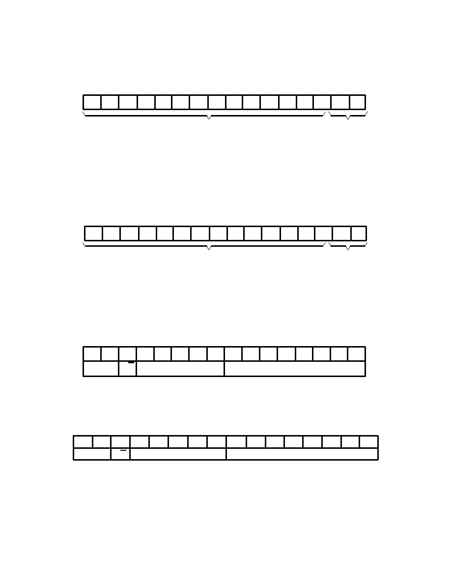
Primary Serial Communications Data Format
D15
D14
D13
D12
D11
D10
D09
D08
D07
D06
D05
D04
D03
D02
D01
D00
14-bit DAC Conversion Result
2s-Complement Format
Control Bits
Since the supply voltage is single ended, the reference for 2s-complement format is ADC VMID. Voltagesabove
this reference have a 0 as the MSB, and voltages below this reference have a 1 as the MSB.
During primary serial communications, when D01 and D00 are both high in the DAC data word to DIN, a
subsequent 16 bits of control information is received by the device at DIN during a secondary
serial-communication interval. This secondary serial-communication interval begins at 1/2 the programmed
conversion time when the B register data value is even or 1/2 the programmed value minus one FCLK when
the B register data value is odd. The time between primary and secondary serial communication is
measured from the falling edge of the primary frame sync to the falling edge of the secondary frame sync
(see Section 2.19 for function and format of control words).
2.18.2
Data Format From DOUT During Primary Serial Communications
14-Bit ADC Conversion Result
2s-Complement Format
D15 is the Sign Bit
D15
D14
D13
D12
D11
D10
D09
D08
D07
D06
D05
D04
D03
D02
D01
D00
D01
+ 0
D00
+ 0
D01
+ 0
D00
+ 1
Master Mode
Slave Mode
2.19 Secondary Serial Communications
2.19.1
Data Format to DIN During Secondary Serial Communications
There are nine 16-bit configuration and control registers numbered from zero to eight. All register data
contents are represented in 2s-complement format. The general format of the commands during secondary
serial communications is as follows.
DS15 DS14 DS13 DS12 DS11 DS10 DS09 DS08 DS07 DS06 DS05 DS04 DS03 DS02 DS01 DS00
Control Bits
(2 bits)
R/W
Bit
Register Address
(5 bits)
Register Data Value
(8 bits)
All control register words are latched in the register and valid on the sixteenth falling edge of SCLK.
2.19.2
Control Data-Bit Function in Secondary Serial Communication
2.19.2.1 DS15 and DS14
In the secondary data word, bits DS15 and DS14 perform the same control function as the primary control
bits D01 and D00 do in the primary data word.
DS15 DS14 DS13 DS12
DS11 DS10 DS09 DS08 DS07 DS06 DS05 DS04 DS03 DS02 DS01 DS00
R/W
Register Address
Register Data
Control Bits
Hardware terminals FC1 and FC0 are valid inputs when DS15 and DS14 are both high, and they are ignored
for all other conditions.
相关PDF资料 |
PDF描述 |
|---|---|
| TLC320AC02IFNR | SPECIALTY ANALOG CIRCUIT, PQCC28 |
| TLC320AD55CDW | SPECIALTY ANALOG CIRCUIT, PDSO28 |
| TLC320AD55CDWR | SPECIALTY ANALOG CIRCUIT, PDSO28 |
| TLC320AD57CDW | 1-CH 18-BIT DELTA-SIGMA ADC, SERIAL ACCESS, PDSO28 |
| TLC320AD57CDWR | 1-CH 18-BIT DELTA-SIGMA ADC, SERIAL ACCESS, PDSO28 |
相关代理商/技术参数 |
参数描述 |
|---|---|
| TLC320AC03CFNG4 | 制造商:Texas Instruments 功能描述: |
| TLC320AC03CFNR | 制造商:Rochester Electronics LLC 功能描述:- Bulk 制造商:Texas Instruments 功能描述: |
| TLC320AC03CPM | 制造商:Rochester Electronics LLC 功能描述:- Bulk 制造商:Texas Instruments 功能描述: |
| TLC320AD50 | 制造商:TI 制造商全称:Texas Instruments 功能描述:SIGMA-DELTA ANALOG INTERFACE CIRCUITS WITH MASTER-SLAVE FUNCTION |
| TLC320AD50C | 制造商:Texas Instruments 功能描述: |
发布紧急采购,3分钟左右您将得到回复。