- 您现在的位置:买卖IC网 > PDF目录98238 > TLC320AC02IPM (TEXAS INSTRUMENTS INC) SPECIALTY ANALOG CIRCUIT, PQFP64 PDF资料下载
参数资料
| 型号: | TLC320AC02IPM |
| 厂商: | TEXAS INSTRUMENTS INC |
| 元件分类: | 模拟信号调理 |
| 英文描述: | SPECIALTY ANALOG CIRCUIT, PQFP64 |
| 封装: | GREEN, PLASTIC, QFP-64 |
| 文件页数: | 3/86页 |
| 文件大小: | 471K |
| 代理商: | TLC320AC02IPM |
第1页第2页当前第3页第4页第5页第6页第7页第8页第9页第10页第11页第12页第13页第14页第15页第16页第17页第18页第19页第20页第21页第22页第23页第24页第25页第26页第27页第28页第29页第30页第31页第32页第33页第34页第35页第36页第37页第38页第39页第40页第41页第42页第43页第44页第45页第46页第47页第48页第49页第50页第51页第52页第53页第54页第55页第56页第57页第58页第59页第60页第61页第62页第63页第64页第65页第66页第67页第68页第69页第70页第71页第72页第73页第74页第75页第76页第77页第78页第79页第80页第81页第82页第83页第84页第85页第86页
1–5
1.4
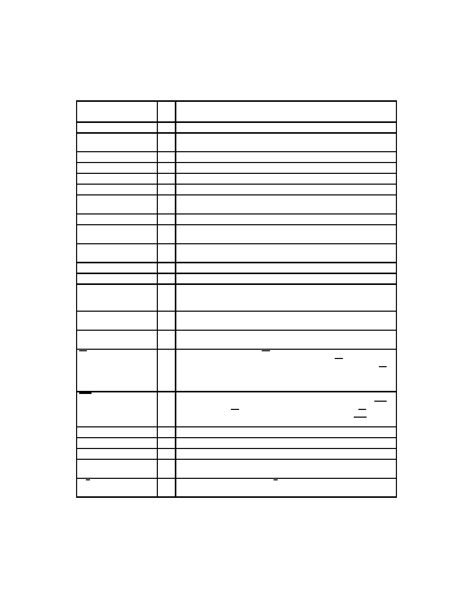
Terminal Functions
TERMINAL
I/O
DESCRIPTION
NAME
NO.
I/O
DESCRIPTION
ADC VDD
24
32
I
Analog supply voltage for the ADC channel
ADC VMID
23
30
O
Midsupply for the ADC channel (requires a bypass capacitor). ADC VMID must be
buffered when used as an external reference.
ADC GND
22
27
I
Analog ground for the ADC channel
AUX IN +
28
38
I
Noninverting input to auxiliary analog input amplifier
AUX IN –
27
37
I
Inverting input to auxiliary analog input amplifier
DAC VDD
5
49
I
Digital supply voltage for the DAC channel
DAC VMID
6
51
O
Midsupply for the DAC channel (requires a bypass capacitor). DAC VMID must be
buffered when used as an external reference.
DAC GND
7
54
I
Analog ground for the DAC channel
DIN
10
1
I
Data input. DIN receives the DAC input data and command information and is
synchronized with SCLK.
DOUT
11
3
O
Data output. DOUT outputs the ADC data results and register read contents.
DOUT is synchronized with SCLK.
DGTL VDD
9
59
I
Digital supply voltage for control logic
DGTL GND
20
22
I
Digital ground for control logic
EOC
19
17
O
End-of-conversion output. EOC goes high at the start of the ADC conversion
period and low when conversion is complete. EOC remains low until the next ADC
conversion period begins and indicates the internal device conversion period.
FC0
15
11
I
Hardware control input. FC0 is used in conjunction with FC1 to request secondary
communication and phase adjustments. FC0 should be tied low if it is not used.
FC1
16
12
I
Hardware control input. FC1 is used in conjunction with FC0 to request secondary
communication and phase adjustments. FC1 should be tied low if it is not used.
FS
12
4
I/O
Frame synchronization. When FS goes low, DIN begins receiving data bits and
DOUT begins transmitting data bits. In master mode, FS is low during the
simultaneous 16-bit transmission to DIN and from DOUT. In slave mode, FS is
externally generated and must be low for one shift-clock period minimum to initiate
the data transfer.
FSD
17
14
O
Frame-synchronization delayed output. This active-low output synchronizes a
slave device to the frame synchronization timing of the master device. FSD is
applied to the slave FS input and is the same duration as the master FS signal but
delayed in time by the number of shift clocks programmed in the FSD register.
IN +
26
36
I
Noninverting input to analog input amplifier
IN –
25
35
I
Inverting input to analog input amplifier
MCLK
14
10
I
The master-clock input drives all the key logic signals of the AIC.
MON OUT
1
40
O
The monitor output allows monitoring of analog input and is a high-impedance
output.
M/S
18
16
I
Master/slave select input. When M/S is high, the device is the master and when
low, it is a slave.
Terminal numbers shown are for the FN package.
Terminal numbers shown are for the PM package.
相关PDF资料 |
PDF描述 |
|---|---|
| TLC320AC02IFNR | SPECIALTY ANALOG CIRCUIT, PQCC28 |
| TLC320AD55CDW | SPECIALTY ANALOG CIRCUIT, PDSO28 |
| TLC320AD55CDWR | SPECIALTY ANALOG CIRCUIT, PDSO28 |
| TLC320AD57CDW | 1-CH 18-BIT DELTA-SIGMA ADC, SERIAL ACCESS, PDSO28 |
| TLC320AD57CDWR | 1-CH 18-BIT DELTA-SIGMA ADC, SERIAL ACCESS, PDSO28 |
相关代理商/技术参数 |
参数描述 |
|---|---|
| TLC320AC03CFNG4 | 制造商:Texas Instruments 功能描述: |
| TLC320AC03CFNR | 制造商:Rochester Electronics LLC 功能描述:- Bulk 制造商:Texas Instruments 功能描述: |
| TLC320AC03CPM | 制造商:Rochester Electronics LLC 功能描述:- Bulk 制造商:Texas Instruments 功能描述: |
| TLC320AD50 | 制造商:TI 制造商全称:Texas Instruments 功能描述:SIGMA-DELTA ANALOG INTERFACE CIRCUITS WITH MASTER-SLAVE FUNCTION |
| TLC320AD50C | 制造商:Texas Instruments 功能描述: |
发布紧急采购,3分钟左右您将得到回复。