- 您现在的位置:买卖IC网 > PDF目录98238 > TLC320AC02IPM (TEXAS INSTRUMENTS INC) SPECIALTY ANALOG CIRCUIT, PQFP64 PDF资料下载
参数资料
| 型号: | TLC320AC02IPM |
| 厂商: | TEXAS INSTRUMENTS INC |
| 元件分类: | 模拟信号调理 |
| 英文描述: | SPECIALTY ANALOG CIRCUIT, PQFP64 |
| 封装: | GREEN, PLASTIC, QFP-64 |
| 文件页数: | 38/86页 |
| 文件大小: | 471K |
| 代理商: | TLC320AC02IPM |
第1页第2页第3页第4页第5页第6页第7页第8页第9页第10页第11页第12页第13页第14页第15页第16页第17页第18页第19页第20页第21页第22页第23页第24页第25页第26页第27页第28页第29页第30页第31页第32页第33页第34页第35页第36页第37页当前第38页第39页第40页第41页第42页第43页第44页第45页第46页第47页第48页第49页第50页第51页第52页第53页第54页第55页第56页第57页第58页第59页第60页第61页第62页第63页第64页第65页第66页第67页第68页第69页第70页第71页第72页第73页第74页第75页第76页第77页第78页第79页第80页第81页第82页第83页第84页第85页第86页
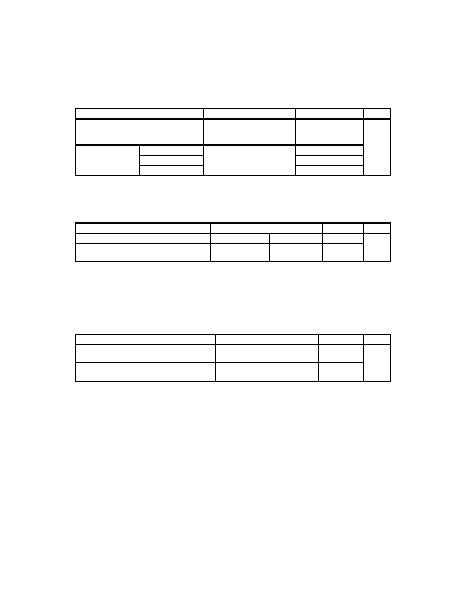
3–5
3.5.7
Noise, Low-Pass and Band-Pass Switched-Capacitor Filters Included,
VDD = 5 V (Unless Otherwise Noted)
PARAMETER
TEST CONDITIONS
MIN
TYP
MAX
UNIT
ADC idle channel noise
Inputs tied to ADC VMID,
f
8 kHz
FCLK
144 kHz
180
300
ADC idle-channel noise
fs = 8 kHz, FCLK = 144 kHz,
(see Note 11)
180
300
DAC idle channel
Broad-band noise
DIN INPUT = 00000000000000,
180
300
Vrms
DAC idle-channel
noise
Noise (0 to 7.2 kHz)
DIN INPUT
00000000000000,
fs = 8 kHz, FCLK = 144 kHz,
(N
)
180
300
noise
Noise (0 to 3.6 kHz)
(see Note 12)
180
300
All typical values are at VDD = 5 V and TA = 25°C.
NOTES: 11. The ADC channel noise is calculated by taking the RMS value of the digital output codes of the ADC
channel and converting to microvolts.
12. The DAC channel noise is measured differentially from OUT + to OUT – across 600
.
3.5.8
Absolute Gain Error, VDD = 5 V, fs = 8 kHz (Unless Otherwise Noted)
PARAMETER
TEST CONDITIONS
MIN
MAX
UNIT
ADC channel absolute gain error (see Note 13)
– 1-dB input signal
TA = –40 – 85°C
±1
DAC channel absolute gain error (see Note 14)
0-dB input signal,
RL = 600
TA = –40 – 85°C
±1
dB
NOTES: 13. ADC absolute gain error is the variation in gain from the ideal gain over the specified input signal levels.
The gain is measured with a – 1-dB, 1020-Hz sine wave. The – 1-dB input signal allows for any positive gain
or offset error that may affect gain measurements at or close to 0-dB input signal levels.
14. The DAC input signal is the digital equivalent of a 1020-Hz sine wave (full-scale analog output at digital full-
scale input = 0 dB). The nominal differential DAC channel output voltage with this input condition is 6 V peak
to peak. The load impedance for the DAC output buffer is 600
from OUT+ to OUT–.
3.5.9
Relative Gain and Dynamic Range, VDD = 5 V, fs = 8 kHz (Unless Otherwise
Noted)
PARAMETER
TEST CONDITIONS
MIN
MAX
UNIT
ADC channel relative gain tracking error
(see Note 15)
– 48-dB to – 1-dB input signal range
±0.2
dB
DAC channel relative gain tracking error
(see Note 16)
– 48-dB to 0-dB input signal range
RL(diff) = 600
±0.2
dB
NOTES: 15. ADC gain tracking is the ratio of the measured gain at one ADC channel input level to the gain measured
at any other input level. The ADC channel input is a –1-dB 1020-Hz sine wave input signal. A –1-dB input
signal allows for any positive gain or offset error that may affect gain measurements at or close to 0-dB ADC
input signal levels.
16. DAC gain tracking is the ratio of the measured gain at one DAC channel digital input level to the gain
measured at any other input level. The DAC-channel input signal is the digital equivalent of a 1020-Hz sine
wave (digital full scale = 0 dB). The nominal differential DAC channel output voltage with this input condition
is 6 V peak to peak. The load impedance for the DAC output buffer is 600
from OUT+ to OUT–.
相关PDF资料 |
PDF描述 |
|---|---|
| TLC320AC02IFNR | SPECIALTY ANALOG CIRCUIT, PQCC28 |
| TLC320AD55CDW | SPECIALTY ANALOG CIRCUIT, PDSO28 |
| TLC320AD55CDWR | SPECIALTY ANALOG CIRCUIT, PDSO28 |
| TLC320AD57CDW | 1-CH 18-BIT DELTA-SIGMA ADC, SERIAL ACCESS, PDSO28 |
| TLC320AD57CDWR | 1-CH 18-BIT DELTA-SIGMA ADC, SERIAL ACCESS, PDSO28 |
相关代理商/技术参数 |
参数描述 |
|---|---|
| TLC320AC03CFNG4 | 制造商:Texas Instruments 功能描述: |
| TLC320AC03CFNR | 制造商:Rochester Electronics LLC 功能描述:- Bulk 制造商:Texas Instruments 功能描述: |
| TLC320AC03CPM | 制造商:Rochester Electronics LLC 功能描述:- Bulk 制造商:Texas Instruments 功能描述: |
| TLC320AD50 | 制造商:TI 制造商全称:Texas Instruments 功能描述:SIGMA-DELTA ANALOG INTERFACE CIRCUITS WITH MASTER-SLAVE FUNCTION |
| TLC320AD50C | 制造商:Texas Instruments 功能描述: |
发布紧急采购,3分钟左右您将得到回复。