- 您现在的位置:买卖IC网 > Datasheet目录367 > TWR-MPC8309 (Freescale Semiconductor)TOWER SYSTEM MODULE MPC8309 Datasheet资料下载
参数资料
| 型号: | TWR-MPC8309 |
| 厂商: | Freescale Semiconductor |
| 文件页数: | 17/81页 |
| 文件大小: | 0K |
| 描述: | TOWER SYSTEM MODULE MPC8309 |
| 设计资源: | TWR-MPC8309 Schematic |
| 标准包装: | 1 |
| 系列: | PowerQUICC II™ PRO |
| 类型: | MPU |
| 适用于相关产品: | Freescale 电源塔系统 |
| 所含物品: | 板,线缆 |
第1页第2页第3页第4页第5页第6页第7页第8页第9页第10页第11页第12页第13页第14页第15页第16页当前第17页第18页第19页第20页第21页第22页第23页第24页第25页第26页第27页第28页第29页第30页第31页第32页第33页第34页第35页第36页第37页第38页第39页第40页第41页第42页第43页第44页第45页第46页第47页第48页第49页第50页第51页第52页第53页第54页第55页第56页第57页第58页第59页第60页第61页第62页第63页第64页第65页第66页第67页第68页第69页第70页第71页第72页第73页第74页第75页第76页第77页第78页第79页第80页第81页
�� �
�
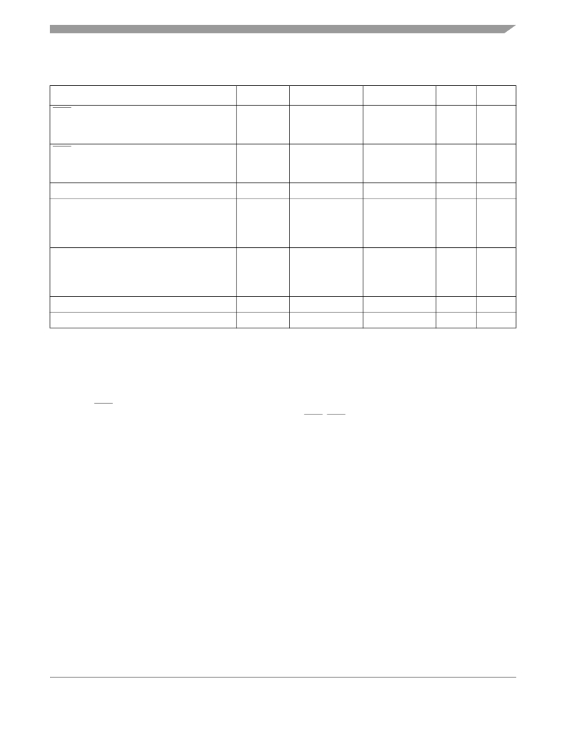
�DDR2� SDRAM�
�Table� 16.� DDR2� SDRAM� output� AC� timing� specifications� (continued)�
�At� recommended� operating� conditions� with� GV� DD� of� 1.8V� ±� 100mV.�
�Parameter�
�MCS� output� setup� with� respect� to� MCK�
�Symbol� 1�
�t� DDKHCS�
�Min�
�Max�
�Unit�
�ns�
�Note�
�3�
�333� MHz�
�266� MHz�
�2.4�
�2.5�
�—�
�MCS� output� hold� with� respect� to� MCK�
�333� MHz�
�266� MHz�
�t� DDKHCX�
�2.4�
�2.5�
�—�
�ns�
�3�
�MCK� to� MDQS� Skew�
�MDQ/MDM� output� setup� with� respect� to� MDQS�
�t� DDKHMH�
�t� DDKHDS,�
�–0.6�
�0.6�
�ns�
�ns�
�4�
�5�
�t� DDKLDS�
�333� MHz�
�266� MHz�
�0.8�
�0.9�
�—�
�MDQ/MDM� output� hold� with� respect� to� MDQS�
�t� DDKHDX,�
�ps�
�5�
�t� DDKLDX�
�333� MHz�
�266� MHz�
�900�
�1100�
�—�
�MDQS� preamble� start�
�MDQS� epilogue� end�
�t� DDKHMP�
�t� DDKHME�
�0.75� x� t� MCK�
�0.4� x� t� MCK�
�—�
�0.6� x� t� MCK�
�ns�
�ns�
�6�
�6�
�Notes:�
�1.� The� symbols� used� for� timing� specifications� follow� the� pattern� of� t� (first� two� letters� of� functional� block)(signal)(state)(reference)(state)� for�
�inputs� and� t� (first� two� letters� of� functional� block)(reference)(state)(signal)(state)� for� outputs.� Output� hold� time� can� be� read� as� DDR� timing�
�(DD)� from� the� rising� or� falling� edge� of� the� reference� clock� (KH� or� KL)� until� the� output� went� invalid� (AX� or� DX).� For� example,�
�t� DDKHAS� symbolizes� DDR� timing� (DD)� for� the� time� t� MCK� memory� clock� reference� (K)� goes� from� the� high� (H)� state� until� outputs�
�(A)� are� setup� (S)� or� output� valid� time.� Also,� t� DDKLDX� symbolizes� DDR� timing� (DD)� for� the� time� t� MCK� memory� clock� reference�
�(K)� goes� low� (L)� until� data� outputs� (D)� are� invalid� (X)� or� data� output� hold� time.�
�2.� All� MCK/MCK� referenced� measurements� are� made� from� the� crossing� of� the� two� signals� ±0.1� V.�
�3.� ADDR/CMD� includes� all� DDR� SDRAM� output� signals� except� MCK/MCK,� MCS,� and� MDQ/MDM/MDQS.� For� the� ADDR/CMD�
�setup� and� hold� specifications,� it� is� assumed� that� the� Clock� Control� register� is� set� to� adjust� the� memory� clocks� by� 1/2� applied�
�cycle.�
�4.� Note� that� t� DDKHMH� follows� the� symbol� conventions� described� in� note� 1.� For� example,� t� DDKHMH� describes� the� DDR� timing� (DD)�
�from� the� rising� edge� of� the� MCK(n)� clock� (KH)� until� the� MDQS� signal� is� valid� (MH).� t� DDKHMH� can� be� modified� through� control�
�of� the� DQSS� override� bits� in� the� TIMING_CFG_2� register.� This� is� typically� set� to� the� same� delay� as� the� clock� adjusts� in� the�
�CLK_CNTL� register.� The� timing� parameters� listed� in� the� table� assume� that� these� 2� parameters� have� been� set� to� the� same�
�adjustment� value.� See� the� MPC8309� PowerQUICC� II� Pro� Integrated� Communications� Processor� Family� Reference� Manual�
�for� a� description� and� understanding� of� the� timing� modifications� enabled� by� use� of� these� bits.�
�5.� Determined� by� maximum� possible� skew� between� a� data� strobe� (MDQS)� and� any� corresponding� bit� of� data� (MDQ),� or� data�
�mask� (MDM).� The� data� strobe� should� be� centered� inside� of� the� data� eye� at� the� pins� of� the� microprocessor.�
�6.� t� DDKHMP� follows� the� symbol� conventions� described� in� note� 1.�
�MPC8309� PowerQUICC� II� Pro� Integrated� Communications� Processor� Family� Hardware� Specifications,� Rev.� 3�
�Freescale� Semiconductor�
�17�
�相关PDF资料 |
PDF描述 |
|---|---|
| TWR-PXN20-KIT | TOWER SYSTEM KIT PXN20 |
| TWR-PXS2010-KIT | TOWER SYSTEM KIT PXS2010 |
| TWR-PXS3020-KIT | TOWER SYSTEM KIT PXS3020 |
| TWR-S08DC-PT60 | TOWER SYSTEM BOARD S08PT60 |
| TWR-S08JE128-KIT | KIT TOWER FOR MC9S08JE |
相关代理商/技术参数 |
参数描述 |
|---|---|
| TWR-P1025 | 功能描述:开发板和工具包 - 其他处理器 TOWER MODULE P1025 RoHS:否 制造商:Freescale Semiconductor 产品:Development Systems 工具用于评估:P3041 核心:e500mc 接口类型:I2C, SPI, USB 工作电源电压: |
| TWR-P1025-KIT | 功能描述:开发板和工具包 - 其他处理器 QORIQ P1 TWR KIT RoHS:否 制造商:Freescale Semiconductor 产品:Development Systems 工具用于评估:P3041 核心:e500mc 接口类型:I2C, SPI, USB 工作电源电压: |
| TWRPI-BLE-DEMO | 功能描述:蓝牙/802.15.1 开发工具 TWRPI-BLE-DEMO RoHS:否 制造商:Panasonic Electronic Components 产品:Bluetooth Evaluation Kit 工具用于评估:PAN1721 频率:2.4 GHz 接口类型:I2C 工作电源电压:2 V to 3.6 V |
| TWRPI-MMA6900 | 功能描述:加速传感器开发工具 MMA6900 SENSOR PLUG-IN RoHS:否 制造商:Murata 工具用于评估:SCA3100-D04 加速:2 g 传感轴:Triple Axis 接口类型:SPI 工作电压:3.3 V |
| TWRPI-MMA845XQ | 功能描述:加速传感器开发工具 Accel TWRPI RoHS:否 制造商:Murata 工具用于评估:SCA3100-D04 加速:2 g 传感轴:Triple Axis 接口类型:SPI 工作电压:3.3 V |
发布紧急采购,3分钟左右您将得到回复。