- 您现在的位置:买卖IC网 > PDF目录275205 > V58C2128804SBT5B (PROMOS TECHNOLOGIES INC) 16M X 8 DDR DRAM, 0.65 ns, PDSO66 PDF资料下载
参数资料
| 型号: | V58C2128804SBT5B |
| 厂商: | PROMOS TECHNOLOGIES INC |
| 元件分类: | DRAM |
| 英文描述: | 16M X 8 DDR DRAM, 0.65 ns, PDSO66 |
| 封装: | 0.400 X 0.875 INCH, PLASTIC, MS-024FC, TSOP2-66 |
| 文件页数: | 11/62页 |
| 文件大小: | 977K |
| 代理商: | V58C2128804SBT5B |
第1页第2页第3页第4页第5页第6页第7页第8页第9页第10页当前第11页第12页第13页第14页第15页第16页第17页第18页第19页第20页第21页第22页第23页第24页第25页第26页第27页第28页第29页第30页第31页第32页第33页第34页第35页第36页第37页第38页第39页第40页第41页第42页第43页第44页第45页第46页第47页第48页第49页第50页第51页第52页第53页第54页第55页第56页第57页第58页第59页第60页第61页第62页
19
ProMOS TECHNOLOGIES
V58C2128(804/404/164)SB
V58C2128(804/404/164)SB Rev. 1.1 March 2004
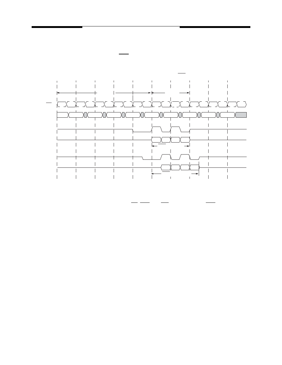
Read Interrupted by a Precharge
A Burst Read operation can be interrupted by a precharge of the same bank. The Precharge command to
Output Disable latency is equivalent to the CAS latency.
Read Interrupted by a Precharge Timing
Burst Write Operation
The Burst Write command is issued by having CS, CAS, and WE low while holding RAS high at the rising
edge of the clock. The address inputs determine the starting column address. The memory controller is re-
quired to provide an input data strobe (DQS) to the DDR SDRAM to strobe or latch the input data (DQ) and
data mask (DM) into the device. During Write cycles, the data strobe applied to the DDR SDRAM is required
to be nominally centered within the data (DQ) and data mask (DM) valid windows. The data strobe must be
driven high nominally one clock after the write command has been registered. Timing parameters tDQSS(min)
and tDQSS(max) define the allowable window when the data strobe must be driven high.
Input data for the first Burst Write cycle must be applied one clock cycle after the Write command is
registered into the device (WL=1). The input data valid window is nominally centered around the midpoint of
the data strobe signal. The data window is defined by DQ to DQS setup time (tQDQSS) and DQ to DQS hold
time (tQDQSH). All data inputs must be supplied on each rising and falling edge of the data strobe until the burst
length is completed. When the burst has finished, any additional data supplied to the DQ pins will be ignored.
Write Preamble and Postamble Operation
Prior to a burst of write data and given that the controller is not currently in burst write mode, the data strobe
signal (DQS), must transition from Hi-Z to a valid logic low. This is referred to as the data strobe “write preamble”.
This transition from Hi-Z to logic low nominally happens on the falling edge of the clock after the write com-
mand has been registered by the device. The preamble is explicitly defined by a setup time (tWPRES(min)) and
hold time (tWPREH(min)) referenced to the first falling edge of CK after the write command.
T0
T1
T2
T3
T4
T5
T6
T7
T8
D0
D1
D2
D3
NOP
Read
NOP
PreA
NOP
BA
NOP
CK, CK
Command
DQS
DQ
tRAS(min)
tRP(min)
BA
NOP
T9
D0
D1
D2
D3
DQS
DQ
CAS Latency=2
CAS Latency=2.5
(CAS Latency = 2, 2.5; Burst Length = 4)
相关PDF资料 |
PDF描述 |
|---|---|
| V59C1256804QAUF25AE | 32M X 8 DDR DRAM, BGA68 |
| V59C1256808QAUF25 | 32M X 8 DDR DRAM, PBGA68 |
| V58C2256324SHUS4E | 8M X 32 DDR DRAM, PBGA60 |
| V58C2256404SHLH4I | 64M X 4 DDR DRAM, PBGA60 |
| V58C2256404SHUB4I | 64M X 4 DDR DRAM, PBGA60 |
相关代理商/技术参数 |
参数描述 |
|---|---|
| V58C2256 | 制造商:MOSEL 制造商全称:MOSEL 功能描述:HIGH PERFORMANCE 2.5 VOLT 256 Mbit DDR SDRAM |
| V58C2256164S | 制造商:MOSEL 制造商全称:MOSEL 功能描述:HIGH PERFORMANCE 2.5 VOLT 256 Mbit DDR SDRAM |
| V58C2256324SAB30 | 制造商:Marvell 功能描述:Marvell V58C2256324SAB30 |
| V58C2256324SAB33 | 制造商:Marvell 功能描述:Marvell V58C2256324SAB33 |
| V58C2256324SAB36 | 制造商:Marvell 功能描述:Marvell V58C2256324SAB36 |
发布紧急采购,3分钟左右您将得到回复。