- 您现在的位置:买卖IC网 > PDF目录275205 > V58C2128804SBT5B (PROMOS TECHNOLOGIES INC) 16M X 8 DDR DRAM, 0.65 ns, PDSO66 PDF资料下载
参数资料
| 型号: | V58C2128804SBT5B |
| 厂商: | PROMOS TECHNOLOGIES INC |
| 元件分类: | DRAM |
| 英文描述: | 16M X 8 DDR DRAM, 0.65 ns, PDSO66 |
| 封装: | 0.400 X 0.875 INCH, PLASTIC, MS-024FC, TSOP2-66 |
| 文件页数: | 5/62页 |
| 文件大小: | 977K |
| 代理商: | V58C2128804SBT5B |
第1页第2页第3页第4页当前第5页第6页第7页第8页第9页第10页第11页第12页第13页第14页第15页第16页第17页第18页第19页第20页第21页第22页第23页第24页第25页第26页第27页第28页第29页第30页第31页第32页第33页第34页第35页第36页第37页第38页第39页第40页第41页第42页第43页第44页第45页第46页第47页第48页第49页第50页第51页第52页第53页第54页第55页第56页第57页第58页第59页第60页第61页第62页
13
ProMOS TECHNOLOGIES
V58C2128(804/404/164)SB
V58C2128(804/404/164)SB Rev. 1.1 March 2004
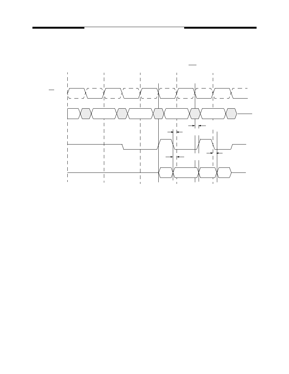
Output Data (DQ) and Data Strobe (DQS) Timing Relative to the Clock (CK)
During Read Cycles
The minimum time during which the output data (DQ) is valid is critical for the receiving device (i.e., a mem-
ory controller device). This also applies to the data strobe during the read cycle since it is tightly coupled to
the output data. The minimum data output valid time (tDV) and minimum data strobe valid time (tDQSV) are de-
rived from the minimum clock high/low time minus a margin for variation in data access and hold time due to
DLL jitter and power supply noise.
(CAS Latency = 2.5; Burst Length = 4)
T0
T1
T2
T3
T4
NOP
D0
CK, CK
Command
DQS
DQ
D2
tDQSCK(max)
tDQSCK(min)
D1
tAC(min)
tAC(max)
D3
READ
NOP
Read Preamble and Postamble Operation
Prior to a burst of read data and given that the controller is not currently in burst read mode, the data strobe
signal (DQS), must transition from Hi-Z to a valid logic low. The is referred to as the data strobe “read pream-
ble” (tRPRE). This transition from Hi-Z to logic low nominally happens one clock cycle prior to the first edge of
valid data.
Once the burst of read data is concluded and given that no subsequent burst read operations are initiated,
the data strobe signal (DQS) transitions from a logic low level back to Hi-Z. This is referred to as the data
strobe “read postamble” (tRPST). This transition happens nominally one-half clock period after the last edge of
valid data.
Consecutive or “gapless” burst read operations are possible from the same DDR SDRAM device with no
requirement for a data strobe “read” preamble or postamble in between the groups of burst data. The data
strobe read preamble is required before the DDR device drives the first output data off chip. Similarly, the
data strobe postamble is initiated when the device stops driving DQ data at the termination of read burst cycles.
相关PDF资料 |
PDF描述 |
|---|---|
| V59C1256804QAUF25AE | 32M X 8 DDR DRAM, BGA68 |
| V59C1256808QAUF25 | 32M X 8 DDR DRAM, PBGA68 |
| V58C2256324SHUS4E | 8M X 32 DDR DRAM, PBGA60 |
| V58C2256404SHLH4I | 64M X 4 DDR DRAM, PBGA60 |
| V58C2256404SHUB4I | 64M X 4 DDR DRAM, PBGA60 |
相关代理商/技术参数 |
参数描述 |
|---|---|
| V58C2256 | 制造商:MOSEL 制造商全称:MOSEL 功能描述:HIGH PERFORMANCE 2.5 VOLT 256 Mbit DDR SDRAM |
| V58C2256164S | 制造商:MOSEL 制造商全称:MOSEL 功能描述:HIGH PERFORMANCE 2.5 VOLT 256 Mbit DDR SDRAM |
| V58C2256324SAB30 | 制造商:Marvell 功能描述:Marvell V58C2256324SAB30 |
| V58C2256324SAB33 | 制造商:Marvell 功能描述:Marvell V58C2256324SAB33 |
| V58C2256324SAB36 | 制造商:Marvell 功能描述:Marvell V58C2256324SAB36 |
发布紧急采购,3分钟左右您将得到回复。