- 您现在的位置:买卖IC网 > PDF目录275205 > V58C2128804SBT5B (PROMOS TECHNOLOGIES INC) 16M X 8 DDR DRAM, 0.65 ns, PDSO66 PDF资料下载
参数资料
| 型号: | V58C2128804SBT5B |
| 厂商: | PROMOS TECHNOLOGIES INC |
| 元件分类: | DRAM |
| 英文描述: | 16M X 8 DDR DRAM, 0.65 ns, PDSO66 |
| 封装: | 0.400 X 0.875 INCH, PLASTIC, MS-024FC, TSOP2-66 |
| 文件页数: | 61/62页 |
| 文件大小: | 977K |
| 代理商: | V58C2128804SBT5B |
第1页第2页第3页第4页第5页第6页第7页第8页第9页第10页第11页第12页第13页第14页第15页第16页第17页第18页第19页第20页第21页第22页第23页第24页第25页第26页第27页第28页第29页第30页第31页第32页第33页第34页第35页第36页第37页第38页第39页第40页第41页第42页第43页第44页第45页第46页第47页第48页第49页第50页第51页第52页第53页第54页第55页第56页第57页第58页第59页第60页当前第61页第62页
8
V58C2128(804/404/164)SB Rev. 1.1 March 2004
ProMOS TECHNOLOGIES
V58C2128(804/404/164)SB
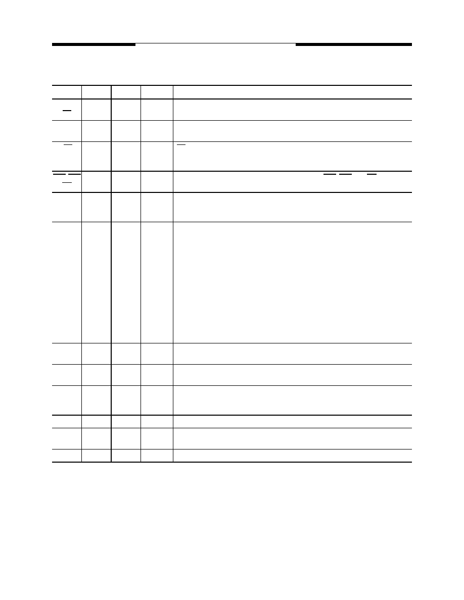
Signal Pin Description
Pin
Type
Signal
Polarity
Function
CK
Input
Pulse
Positive
Edge
The system clock input. All inputs except DQs and DMs are sampled on the rising edge
of CK.
CKE
Input
Level
Active High Activates the CK signal when high and deactivates the CK signal when low, thereby ini-
tiates either the Power Down mode, or the Self Refresh mode.
CS
Input
Pulse
Active Low CS enables the command decoder when low and disables the command decoder when
high. When the command decoder is disabled, new commands are ignored but previous
operations continue.
RAS, CAS
WE
Input
Pulse
Active Low When sampled at the positive rising edge of the clock, CAS, RAS, and WE define the
command to be executed by the SDRAM.
DQS
Input/
Output
Pulse
Active High Active on both edges for data input and output.
Center aligned to input data
Edge aligned to output data
A0 - A11
Input
Level
—
During a Bank Activate command cycle, A0-A11 defines the row address (RA0-RA11)
when sampled at the rising clock edge.
During a Read or Write command cycle, A0-An defines the column address (CA0-CAn)
when sampled at the rising clock edge.CAn depends on the SDRAM organization:
32M x 4 DDR CAn = CA9, A11
16M x 8 DDR CAn = CA9
8M x 16 DDR CAn = CA8
In addition to the column address, A10(=AP) is used to invoke autoprecharge operation
at the end of the burst read or write cycle. If A10 is high, autoprecharge is selected and
BA0, BA1 defines the bank to be precharged. If A10 is low, autoprecharge is disabled.
During a Precharge command cycle, A10(=AP) is used in conjunction with BA0 and BA1
to control which bank(s) to precharge. If A10 is high, all four banks will be precharged
simultaneously regardless of state of BA0 and BA1.
BA0,
BA1
Input
Level
—
Selects which bank is to be active.
DQx
Input/
Output
Level
—
Data Input/Output pins operate in the same manner as on conventional DRAMs.
DM,
LDM,
UDM
Input
Pulse
Active High In Write mode, DM has a latency of zero and operates as a word mask by allowing input
data to be written if it is low but blocks the write operation if is high for x 16 LDM
corresponds to data on DQ0-DQ7, UDM corresponds to data on DQ8-DQ15.
VDD, VSS
Supply
Power and ground for the input buffers and the core logic.
VDDQ
VSSQ
Supply
—
Isolated power supply and ground for the output buffers to provide improved noise
immunity.
VREF
Input
Level
—
SSTL Reference Voltage for Inputs
相关PDF资料 |
PDF描述 |
|---|---|
| V59C1256804QAUF25AE | 32M X 8 DDR DRAM, BGA68 |
| V59C1256808QAUF25 | 32M X 8 DDR DRAM, PBGA68 |
| V58C2256324SHUS4E | 8M X 32 DDR DRAM, PBGA60 |
| V58C2256404SHLH4I | 64M X 4 DDR DRAM, PBGA60 |
| V58C2256404SHUB4I | 64M X 4 DDR DRAM, PBGA60 |
相关代理商/技术参数 |
参数描述 |
|---|---|
| V58C2256 | 制造商:MOSEL 制造商全称:MOSEL 功能描述:HIGH PERFORMANCE 2.5 VOLT 256 Mbit DDR SDRAM |
| V58C2256164S | 制造商:MOSEL 制造商全称:MOSEL 功能描述:HIGH PERFORMANCE 2.5 VOLT 256 Mbit DDR SDRAM |
| V58C2256324SAB30 | 制造商:Marvell 功能描述:Marvell V58C2256324SAB30 |
| V58C2256324SAB33 | 制造商:Marvell 功能描述:Marvell V58C2256324SAB33 |
| V58C2256324SAB36 | 制造商:Marvell 功能描述:Marvell V58C2256324SAB36 |
发布紧急采购,3分钟左右您将得到回复。