- 您现在的位置:买卖IC网 > PDF目录141434 > W25Q128BVFIG (WINBOND ELECTRONICS CORP) 128M X 1 SPI BUS SERIAL EEPROM, PDSO16 PDF资料下载
参数资料
| 型号: | W25Q128BVFIG |
| 厂商: | WINBOND ELECTRONICS CORP |
| 元件分类: | PROM |
| 英文描述: | 128M X 1 SPI BUS SERIAL EEPROM, PDSO16 |
| 封装: | 0.300 INCH, GREEN, SOIC-16 |
| 文件页数: | 58/74页 |
| 文件大小: | 855K |
| 代理商: | W25Q128BVFIG |
第1页第2页第3页第4页第5页第6页第7页第8页第9页第10页第11页第12页第13页第14页第15页第16页第17页第18页第19页第20页第21页第22页第23页第24页第25页第26页第27页第28页第29页第30页第31页第32页第33页第34页第35页第36页第37页第38页第39页第40页第41页第42页第43页第44页第45页第46页第47页第48页第49页第50页第51页第52页第53页第54页第55页第56页第57页当前第58页第59页第60页第61页第62页第63页第64页第65页第66页第67页第68页第69页第70页第71页第72页第73页第74页
W25Q128BV
Publication Release Date: April 01, 2011
- 61 -
Revision E
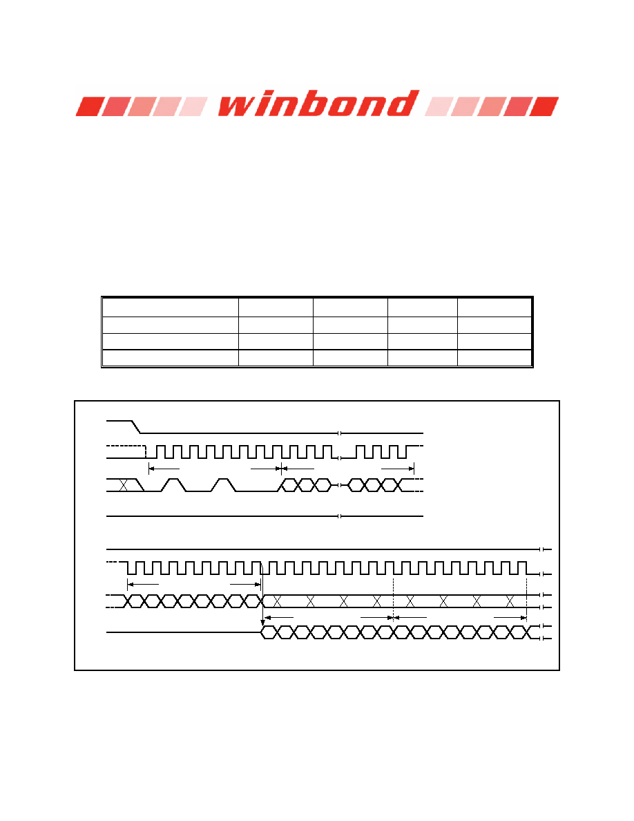
7.2.39 Read Security Registers (48h)
The Read Security Register instruction is similar to the Fast Read instruction and allows one or more data
bytes to be sequentially read from one of the three security registers. The instruction is initiated by driving
the /CS pin low and then shifting the instruction code “48h” followed by a 24-bit address (A23-A0) and
eight “dummy” clocks into the DI pin. The code and address bits are latched on the rising edge of the CLK
pin. After the address is received, the data byte of the addressed memory location will be shifted out on
the DO pin at the falling edge of CLK with most significant bit (MSB) first. The byte address is
automatically incremented to the next byte address after each byte of data is shifted out. Once the byte
address reaches the last byte of the register (byte FFh), it will reset to 00h, the first byte of the register,
and continue to increment. The instruction is completed by driving /CS high. The Read Security Register
instruction sequence is shown in Figure 37. If a Read Security Register instruction is issued while an
Erase, Program or Write cycle is in process (BUSY=1) the instruction is ignored and will not have any
effects on the current cycle. The Read Security Register instruction allows clock rates from D.C. to a
maximum of FR (see AC Electrical Characteristics).
ADDRESS
A23-16
A15-12
A11-8
A7-0
Security Register #1
00h
0 0 0 1
0 0 0 0
Byte Address
Security Register #2
00h
0 0 1 0
0 0 0 0
Byte Address
Security Register #3
00h
0 0 1 1
0 0 0 0
Byte Address
/CS
CLK
DI
(IO
0)
DO
(IO
1)
Mode 0
Mode 3
0
1
2
3
4
5
6
7
Instruction (48h)
High Impedance
8
9
10
28
29
30
31
24-Bit Address
23
22
21
3
2
1
0
Data Out 1
*
/CS
CLK
DI
(IO
0)
DO
32
(IO
1)
33
34
35
36
37
38
39
Dummy Byte
High Impedance
40
41
42
44
45
46
47
48
49
50
51
52
53
54
55
7
6
5
4
3
2
1
0
7
Data Out 2
*
7
6
5
4
3
2
1
0
*
7
6
5
4
3
2
1
0
43
31
0
= MSB
*
Figure 37. Read Security Registers Instruction Sequence
相关PDF资料 |
PDF描述 |
|---|---|
| W7NCF08GH10ISBEG | 512M X 16 FLASH 3.3V PROM CARD, 150 ns, UUC |
| W7NCF08GH10ISBFG | 512M X 16 FLASH 3.3V PROM CARD, 150 ns, UUC |
| W7NCF08GH31CS4JG | 512M X 16 FLASH 3.3V PROM CARD, 150 ns, UUC |
| W7NCF08GH31CS6EG | 512M X 16 FLASH 3.3V PROM CARD, 150 ns, UUC |
| W7NCF128H21CS3HG | 8M X 16 FLASH 3.3V PROM CARD, 150 ns, UUC |
相关代理商/技术参数 |
参数描述 |
|---|---|
| W25Q128BVFIP | 制造商:WINBOND 制造商全称:Winbond 功能描述:3V 128M-BIT SERIAL FLASH MEMORY WITH DUAL AND QUAD SPI |
| W25Q128FV | 制造商:WINBOND 制造商全称:Winbond 功能描述:SERIAL FLASH MEMORY WITH DUAL/QUAD SPI & QPI |
| W25Q128FVAIG | 制造商:WINBOND 制造商全称:Winbond 功能描述:3V 128M-BIT SERIAL FLASH MEMORY WITH DUAL/QUAD SPI & QPI |
| W25Q128FVAIP | 制造商:WINBOND 制造商全称:Winbond 功能描述:3V 128M-BIT SERIAL FLASH MEMORY WITH DUAL/QUAD SPI & QPI |
| W25Q128FVAIQ | 制造商:WINBOND 制造商全称:Winbond 功能描述:3V 128M-BIT SERIAL FLASH MEMORY WITH DUAL/QUAD SPI & QPI |
发布紧急采购,3分钟左右您将得到回复。