- 您现在的位置:买卖IC网 > PDF目录231502 > W3E32M72S-266BC (WHITE ELECTRONIC DESIGNS CORP) 32M X 72 DDR DRAM, 0.75 ns, PBGA219 PDF资料下载
参数资料
| 型号: | W3E32M72S-266BC |
| 厂商: | WHITE ELECTRONIC DESIGNS CORP |
| 元件分类: | DRAM |
| 英文描述: | 32M X 72 DDR DRAM, 0.75 ns, PBGA219 |
| 封装: | 32 X 25 MM, PLASTIC, BGA-219 |
| 文件页数: | 14/19页 |
| 文件大小: | 739K |
| 代理商: | W3E32M72S-266BC |
W3E32M72S-XBX
4
White Electronic Designs Corporation (602) 437-1520 www.whiteedc.com
White Electronic Designs
March 2006
Rev. 2
White Electronic Designs Corp. reserves the right to change products or specications without notice.
A0-12
BA0-1
CK0#CK#
DQ0
DQ15
CKEB
CKE
DM0
DQML
DM1
DQMH
DQ0
DQ15
U1
A0-12
BA0-1
CK1#CK#
16
DQ31
RASB#
WEB#
CASB#
DQ0
DQ15
U0
CKEB
CKE
DM2
DQML
DM3
DQMH
DQ0
DQ15
U2
A0-12
BA0-1
CK2#CK#
DQ32
DQ47
CKEB
CKE
DM4
DQML
DM5
DQMH
DQ0
DQ15
U3
A0-12
BA0-1
CK3#CK#
DQ48
DQ63
CKEB
CKE
DQS6
DQSL
DQS7
DQSH
DQ0
DQ15
U4
A0-12
BA0-1
CK4#CK#
DQ64
DQ79
CKEB
CKE
DQS8
DQSL
DQS9
DQSH
Y
=
Y
=
Y
=
Y
=
Y
=
Y
=
Y
=
Y
=
Y
=
Y
=
Y
=
Y
=
DQ
Y
=
Y
=
Y
=
Y
=
Y
=
Y
=
Y
=
Y
=
Y
=
Y
=
Y
=
Y
=
Y
=
Y
=
Y
=
Y
=
Y
=
Y
=
Y
=
Y
=
Y
=
Y
=
Y
=
Y
=
Y
=
Y
=
Y
=
Y
=
Y
=
Y
=
Y
=
Y
=
Y
=
Y
=
Y
=
Y
=
Y
=
Y
=
Y
=
Y
=
Y
=
Y
=
Y
=
Y
=
Y
=
Y
=
Y
=
Y
=
CK4
CK
VREF
CK3
CK
VREF
DQS4
DQSL
DQS5
DQSH
VREF
DQS2
DQSL
DQS3
DQSH
VREF
DQS0
DQSL
DQS1
DQSH
VREF
CK2
CK
CK1
CK
CK0
CK
VREF
DM6
DQML
DM7
DQMH
DM8
DM9
DQML
DQMH
A0-12
BA0-1
CSB#
CAS#
WE# RAS#
CS#
CAS#
WE# RAS#
CS#
CAS#
WE# RAS#
CS#
CAS#
WE# RAS#
CS#
CAS#
WE# RAS#
CS#
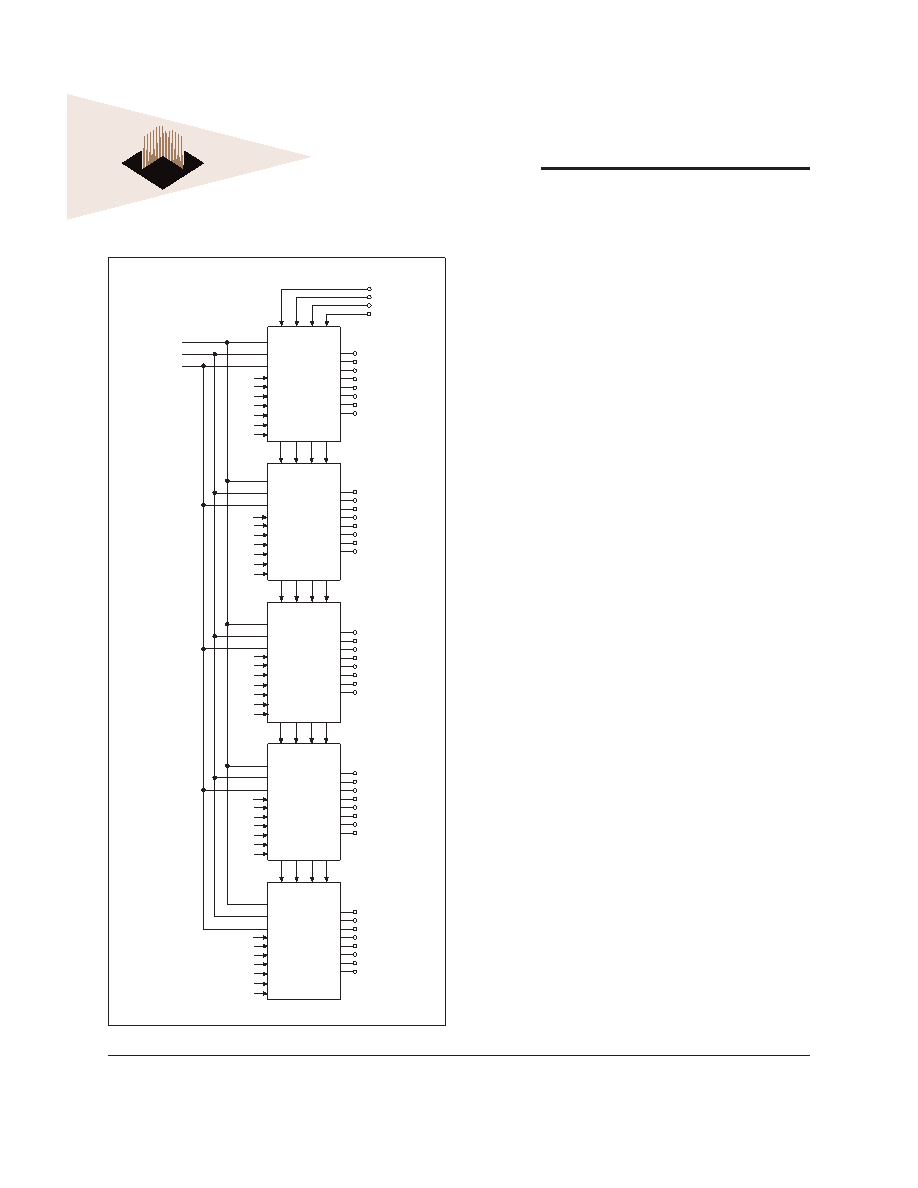
FIGURE 2 – FUNCTIONAL BLOCK DIAGRAM
after VCCQ to avoid device latch-up, which may cause
permanent damage to the device. VREF can be applied any
time after VCCQ but is expected to be nominally coincident
with VTT. Except for CKE, inputs are not recognized as
valid until after VREF is applied. CKE is an SSTL_2
input but will detect an LVCMOS LOW level after VCC is
applied. After CKE passes through VIH, it will transition to
an SSTL_2 signal and remain as such until power is cycled.
Maintaining an LVCMOS LOW level on CKE during power-
up is required to ensure that the DQ and DQS outputs will
be in the High-Z state, where they will remain until driven
in normal operation (by a read access). After all power
supply and reference voltages are stable, and the clock
is stable, the DDR SDRAM requires a 200μs delay prior
to applying an executable command.
Once the 200μs delay has been satised, a DESELECT
or NOP command should be applied, and CKE should
be brought HIGH. Following the NOP command, a
PRECHARGE ALL command should be applied. Next a
LOAD MODE REGISTER command should be issued for
the extended mode register (BA1 LOW and BA0 HIGH)
to enable the DLL, followed by another LOAD MODE
REGISTER command to the mode register (BA0/BA1
both LOW) to reset the DLL and to program the operating
parameters. Two-hundred clock cycles are required
between the DLL reset and any READ command. A
PRECHARGE ALL command should then be applied,
placing the device in the all banks idle state.
Once in the idle state, two AUTO REFRESH cycles must
be performed (tRFC must be satised.) Additionally, a LOAD
MODE REGISTER command for the mode register with
the reset DLL bit deactivated (i.e., to program operating
parameters without resetting the DLL) is required.
Following these requirements, the DDR SDRAM is ready
for normal operation.
相关PDF资料 |
PDF描述 |
|---|---|
| W3HG128M72AEF665F1MCG | DDR DRAM MODULE, DMA240 |
| WS128K32-100G4QE | 512K X 8 MULTI DEVICE SRAM MODULE, 100 ns, CQFP68 |
| WS128K32N-70HME | 512K X 8 MULTI DEVICE SRAM MODULE, 70 ns, CHIP66 |
| WPS512K32-15PJI | 2M X 8 MULTI DEVICE SRAM MODULE, 15 ns, PQMA68 |
| WMD4M4V-80F2M | 4M X 4 FAST PAGE DRAM, 80 ns, CDSO24 |
相关代理商/技术参数 |
参数描述 |
|---|---|
| W3E32M72S-266BI | 制造商:Microsemi Corporation 功能描述:32M X 72 DDR, 2.5V, 266 MHZ, 219 PBGA, INDUSTRIAL TEMP. - Bulk |
| W3E32M72S-266BM | 制造商:Microsemi Corporation 功能描述:32M X 72 DDR, 2.5V, 266 MHZ, 219 PBGA, MIL-TEMP. - Bulk |
| W3E32M72S-266SBC | 制造商:Microsemi Corporation 功能描述:32M X 72 DDR, 2.5V, 266 MHZ, 208 PBGA, COMMERCIAL TEMP. - Bulk |
| W3E32M72S-266SBI | 制造商:White Electronic Designs 功能描述:32M X 72 DDR, 2.5V, 266 MHZ, 208 PBGA, IND TEMP CUSTOM - Bulk 制造商:Microsemi Corporation 功能描述:SDRAM MEMORY |
| W3E32M72S-266SBM | 制造商:WEDC 制造商全称:White Electronic Designs Corporation 功能描述:32Mx72 DDR SDRAM |
发布紧急采购,3分钟左右您将得到回复。