- 您现在的位置:买卖IC网 > PDF目录231502 > W3E32M72S-266BC (WHITE ELECTRONIC DESIGNS CORP) 32M X 72 DDR DRAM, 0.75 ns, PBGA219 PDF资料下载
参数资料
| 型号: | W3E32M72S-266BC |
| 厂商: | WHITE ELECTRONIC DESIGNS CORP |
| 元件分类: | DRAM |
| 英文描述: | 32M X 72 DDR DRAM, 0.75 ns, PBGA219 |
| 封装: | 32 X 25 MM, PLASTIC, BGA-219 |
| 文件页数: | 17/19页 |
| 文件大小: | 739K |
| 代理商: | W3E32M72S-266BC |
W3E32M72S-XBX
7
White Electronic Designs Corporation (602) 437-1520 www.whiteedc.com
White Electronic Designs
March 2006
Rev. 2
White Electronic Designs Corp. reserves the right to change products or specications without notice.
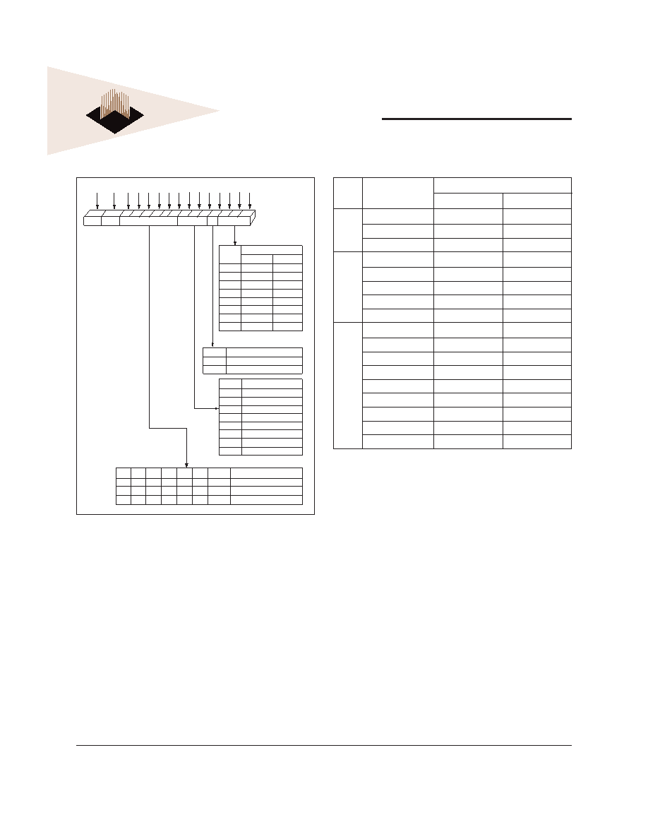
TABLE 1 – BURST DEFINITION
Burst
Length
Starting Column
Address
Order of Accesses Within a Burst
Type = Sequential
Type = Interleaved
2
A0
0
0-1
1
1-0
4
A1
A0
0
0-1-2-3
0
1
1-2-3-0
1-0-3-2
1
0
2-3-0-1
1
3-0-1-2
3-2-1-0
8
A2
A1
A0
0
0-1-2-3-4-5-6-7
0
1
1-2-3-4-5-6-7-0
1-0-3-2-5-4-7-6
0
1
0
2-3-4-5-6-7-0-1
2-3-0-1-6-7-4-5
0
1
3-4-5-6-7-0-1-2
3-2-1-0-7-6-5-4
1
0
4-5-6-7-0-1-2-3
1
0
1
5-6-7-0-1-2-3-4
5-4-7-6-1-0-3-2
1
0
6-7-0-1-2-3-4-5
6-7-4-5-2-3-0-1
1
7-0-1-2-3-4-5-6
7-6-5-4-3-2-1-0
NOTES:
1. For a burst length of two, A1-Ai select two-data-element block; A0
selects the starting column within the block.
2. For a burst length of four, A2-Ai select four-data-element block; A0-1
select the starting column within the block.
3. For a burst length of eight, A3-Ai select eight-data-element block;
A0-2 select the starting column within the block.
4. Whenever a boundary of the block is reached within a given
sequence above, the following access wraps within the block.
FIGURE 3 – MODE REGISTER DEFINITION
M3 = 0
2
4
8
Reserved
M3 = 1
2
4
8
Reserved
Operating Mode
Normal Operation
Normal Operation/Reset DLL
All other states reserved
00
Valid
0
1
Burst Type
Sequential
Interleaved
CAS Latency
Reserved
2
Reserved
2.5
Reserved
Burst Length
M0
0
1
0
1
0
1
0
1
Burst Length
CAS Latency
BT
A9
A7
A6
A5
A4
A3
A8
A2
A1
A0
Mode Register (Mx)
Address Bus
M1
0
1
0
1
M2
0
1
M3
M4
0
1
0
1
0
1
0
1
M5
0
1
0
1
M6
0
1
M6-M0
M8
M7
Operating Mode
A10
A11
* M14 and M13
(BA0 and BA1 must be
"0, 0" to select
the base mode register
(vs. the extended
mode register).
0*
BA0
BA1
Reserved
M9
M10
M11
0
10
0
--
-
A12
M12
0
-
14
13
12 11 10
9
8
7
6
5
4
3
2
1
0
WRITE
The WRITE command is used to initiate a burst write
access to an active row. The value on the BA0, BA1 inputs
selects the bank, and the address provided on inputs A0-9
selects the starting column location. The value on input A10
determines whether or not AUTO PRECHARGE is used. If
AUTO PRECHARGE is selected, the row being accessed
will be precharged at the end of the WRITE burst; if AUTO
PRECHARGE is not selected, the row will remain open
for subsequent accesses. Input data appearing on the DQ
is written to the memory array subject to the DQM input
logic level appearing coincident with the data. If a given
DQM signal is registered LOW, the corresponding data
will be written to memory; if the DQM signal is registered
HIGH, the corresponding data inputs will be ignored, and a
WRITE will not be executed to that byte/column location.
PRECHARGE
The PRECHARGE command is used to deactivate the
open row in a particular bank or the open row in all banks.
The bank(s) will be available for a subsequent row access
a specied time (tRP) after the PRECHARGE command is
issued. Except in the case of concurrent auto precharge,
where a READ or WRITE command to a different bank is
allowed as long as it does not interrupt the data transfer
in the current bank and does not violate any other timing
parameters. Input A10 determines whether one or all
banks are to be precharged, and in the case where only
one bank is to be precharged, inputs BA0, BA1 select the
bank. Otherwise BA0, BA1 are treated as “Don’t Care.”
Once a bank has been precharged, it is in the idle state and
相关PDF资料 |
PDF描述 |
|---|---|
| W3HG128M72AEF665F1MCG | DDR DRAM MODULE, DMA240 |
| WS128K32-100G4QE | 512K X 8 MULTI DEVICE SRAM MODULE, 100 ns, CQFP68 |
| WS128K32N-70HME | 512K X 8 MULTI DEVICE SRAM MODULE, 70 ns, CHIP66 |
| WPS512K32-15PJI | 2M X 8 MULTI DEVICE SRAM MODULE, 15 ns, PQMA68 |
| WMD4M4V-80F2M | 4M X 4 FAST PAGE DRAM, 80 ns, CDSO24 |
相关代理商/技术参数 |
参数描述 |
|---|---|
| W3E32M72S-266BI | 制造商:Microsemi Corporation 功能描述:32M X 72 DDR, 2.5V, 266 MHZ, 219 PBGA, INDUSTRIAL TEMP. - Bulk |
| W3E32M72S-266BM | 制造商:Microsemi Corporation 功能描述:32M X 72 DDR, 2.5V, 266 MHZ, 219 PBGA, MIL-TEMP. - Bulk |
| W3E32M72S-266SBC | 制造商:Microsemi Corporation 功能描述:32M X 72 DDR, 2.5V, 266 MHZ, 208 PBGA, COMMERCIAL TEMP. - Bulk |
| W3E32M72S-266SBI | 制造商:White Electronic Designs 功能描述:32M X 72 DDR, 2.5V, 266 MHZ, 208 PBGA, IND TEMP CUSTOM - Bulk 制造商:Microsemi Corporation 功能描述:SDRAM MEMORY |
| W3E32M72S-266SBM | 制造商:WEDC 制造商全称:White Electronic Designs Corporation 功能描述:32Mx72 DDR SDRAM |
发布紧急采购,3分钟左右您将得到回复。