- 您现在的位置:买卖IC网 > PDF目录300103 > W9425G6EB-6I (WINBOND ELECTRONICS CORP) 16M X 16 DDR DRAM, 0.7 ns, PBGA60 PDF资料下载
参数资料
| 型号: | W9425G6EB-6I |
| 厂商: | WINBOND ELECTRONICS CORP |
| 元件分类: | DRAM |
| 英文描述: | 16M X 16 DDR DRAM, 0.7 ns, PBGA60 |
| 封装: | 8 X 13 MM, ROHS COMPLIANT, TFBGA-60 |
| 文件页数: | 49/51页 |
| 文件大小: | 2017K |
| 代理商: | W9425G6EB-6I |
第1页第2页第3页第4页第5页第6页第7页第8页第9页第10页第11页第12页第13页第14页第15页第16页第17页第18页第19页第20页第21页第22页第23页第24页第25页第26页第27页第28页第29页第30页第31页第32页第33页第34页第35页第36页第37页第38页第39页第40页第41页第42页第43页第44页第45页第46页第47页第48页当前第49页第50页第51页
W9425G6EB
Publication Release Date:Feb. 12, 2009
- 7 -
Revision A02
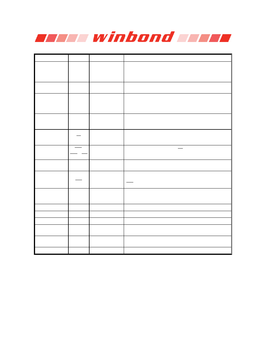
5. BALL DESCRIPTION
BALL NUMBER SYMBOL
FUNCTION
DESCRIPTION
K7, L8, L7, M8,
M2, L3, L2, K3,
K2, J3, K8, J2, H2
A0
A12
Address
Multiplexed pins for row and column address.
Row address: A0
A12.
Column address: A0
A8. (A10 is used for Auto-precharge)
J8, J7
BA0, BA1
Bank Select
Select bank to activate during row address latch time, or
bank to read/write during column address latch time.
A8, B9, B7, C9,
C7, D9, D7, E9,
E1, D3, D1, C3,
C1, B3, B1, A2
DQ0
DQ15
Data Input/ Output
The DQ0 – DQ15 input and output data are synchronized
with both edges of DQS.
E7, E3
LDQS,
UDQS
Data Strobe
DQS is Bi-directional signal. DQS is input signal during write
operation and output signal during read operation. It is Edge-
aligned with read data, Center-aligned with write data.
H8
CS
Chip Select
Disable or enable the command decoder. When command
decoder is disabled, new command is ignored and previous
operation continues.
H7, G8, G7
RAS ,
CAS , WE
Command Inputs Command inputs (along with CS ) define the command
being entered.
F7, F3
LDM, UDM
Write Mask
When DM is asserted “high” in burst write, the input data is
masked. DM is synchronized with both edges of DQS.
G2, G3
CLK,
CLK
Differential Clock
Inputs
All address and control input signals are sampled on the
crossing of the positive edge of CLK and negative edge of
CLK
.
H3
CKE
Clock Enable
CKE controls the clock activation and deactivation. When
CKE is low, Power Down mode, Suspend mode, or Self
Refresh mode is entered.
F1
VREF
Reference Voltage VREF is reference voltage for inputs.
F8, M7, A7
VDD
Power (+2.5V)
Power for logic circuit inside DDR SDRAM.
A3, F2, M3
VSS
Ground
Ground for logic circuit inside DDR SDRAM.
B2, D2, C8, E8,
A9
VDDQ
Power (+2.5V) for
I/O Buffer
Separated power from VDD, used for output buffer, to
improve noise.
A1, C2, E2, B8,
D8
VSSQ
Ground for I/O
Buffer
Separated ground from VSS, used for output buffer, to
improve noise.
F9
NC
No Connection
No connection
相关PDF资料 |
PDF描述 |
|---|---|
| W965L6ABN80I | 2M X 16 PSEUDO STATIC RAM, 75 ns, PBGA48 |
| W9712G6JB-3 | 8M X 16 DDR DRAM, 0.45 ns, PBGA84 |
| W981616CH-5 | 1M X 16 SYNCHRONOUS DRAM, 5.5 ns, PDSO50 |
| W986408AH-10 | 8M X 8 SYNCHRONOUS DRAM, 8 ns, PDSO54 |
| W986408BH-8N | 8M X 8 SYNCHRONOUS DRAM, 6 ns, PDSO54 |
相关代理商/技术参数 |
参数描述 |
|---|---|
| W9425G6EH | 制造商:WINBOND 制造商全称:Winbond 功能描述:4 M 】 4 BANKS 】 16 BITS DDR SDRAM |
| W9425G6EH_0812 | 制造商:WINBOND 制造商全称:Winbond 功能描述:4 M × 4 BANKS × 16 BITS DDR SDRAM |
| W9425G6EH-5 | 功能描述:IC DDR-400 SDRAM 256MB 66TSSOPII RoHS:是 类别:集成电路 (IC) >> 存储器 系列:- 标准包装:1,000 系列:- 格式 - 存储器:EEPROMs - 串行 存储器类型:EEPROM 存储容量:4K (512 x 8) 速度:400kHz 接口:I²C,2 线串口 电源电压:2.7 V ~ 5.5 V 工作温度:-40°C ~ 85°C 封装/外壳:8-SOIC(0.173",4.40mm 宽) 供应商设备封装:8-MFP 包装:带卷 (TR) |
| W9425G6EH-5I | 制造商:Winbond Electronics Corp 功能描述: |
| W9425G6JB-5 | 制造商:Winbond Electronics Corp 功能描述:DRAM Chip DDR SDRAM 256M-Bit 16Mx16 2.5V 60-Pin TFBGA 制造商:Winbond Electronics 功能描述:IC MEMORY 制造商:Winbond Electronics Corp 功能描述:IC MEMORY 制造商:Winbond 功能描述:16MX16,256Mb DDRI DRAM ,200MHZ, BGA |
发布紧急采购,3分钟左右您将得到回复。