- 您现在的位置:买卖IC网 > PDF目录231501 > W981216DH-75 (WINBOND ELECTRONICS CORP) 8M X 16 SYNCHRONOUS DRAM, 5.4 ns, PDSO54 PDF资料下载
参数资料
| 型号: | W981216DH-75 |
| 厂商: | WINBOND ELECTRONICS CORP |
| 元件分类: | DRAM |
| 英文描述: | 8M X 16 SYNCHRONOUS DRAM, 5.4 ns, PDSO54 |
| 封装: | 0.400 INCH, 0.80 MM PITCH, TSOP2-54 |
| 文件页数: | 8/44页 |
| 文件大小: | 1221K |
| 代理商: | W981216DH-75 |
第1页第2页第3页第4页第5页第6页第7页当前第8页第9页第10页第11页第12页第13页第14页第15页第16页第17页第18页第19页第20页第21页第22页第23页第24页第25页第26页第27页第28页第29页第30页第31页第32页第33页第34页第35页第36页第37页第38页第39页第40页第41页第42页第43页第44页

W981216DH / W9812G6DH
- 16 -
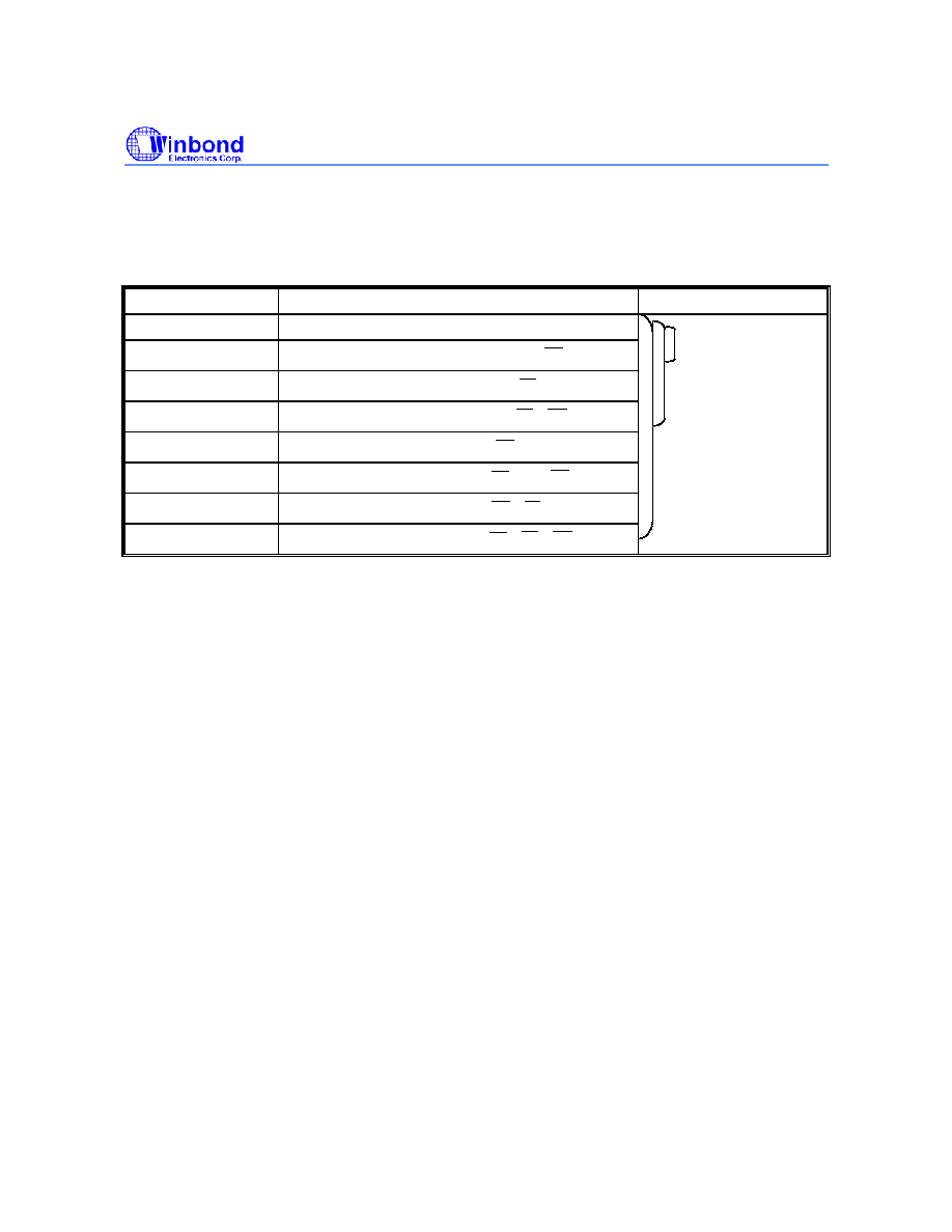
12.13 Addressing Sequence of Interleave Mode
A column access is started in the input column address and is performed by inverting the address bit
in the sequence shown in Table 3.
Table 3 Address Sequence of Interleave Mode
DATA
ACCESS ADDRESS
BUST LENGTH
Data 0
A8 A7 A6 A5 A4 A3 A2 A1 A0
BL = 2
Data 1
A8 A7 A6 A5 A4 A3 A2 A1 A0
Data 2
A8 A7 A6 A5 A4 A3 A2 A1 A0
BL = 4
Data 3
A8 A7 A6 A5 A4 A3 A2 A1 A0
Data 4
A8 A7 A6 A5 A4 A3 A2 A1 A0
BL = 8
Data 5
A8 A7 A6 A5 A4 A3 A2 A1 A0
Data 6
A8 A7 A6 A5 A4 A3 A2 A1 A0
Data 7
A8 A7 A6 A5 A4 A3 A2 A1 A0
12.14 Auto-Precharge Command
If A10 is set to high when the Read or Write Command is issued, then the auto-precharge function is
entered. During auto-precharge, a Read Command will execute as normal with the exception that the
active bank will begin to precharge automatically before all burst read cycles have been completed.
Regardless of burst length, it will begin a certain number of clocks prior to the end of the scheduled
burst cycle. The number of clocks is determined by CAS latency.
A Read or Write Command with auto-precharge can not be interrupted before the entire burst
operation is completed. Therefore, use of a Read, Write, or Precharge Command is prohibited during
a read or write cycle with auto-precharge. Once the precharge operation has started, the bank cannot
be reactivated until the Precharge time (tRP) has been satisfied. Issue of Auto-Precharge command is
illegal if the burst is set to full page length. If A10 is high when a Write Command is issued, the Write
with Auto-Precharge function is initiated. The SDRAM automatically enters the precharge operation
two clocks delay from the last burst write cycle. This delay is referred to as Write tWR. The bank
undergoing auto-precharge can not be reactivated until tWR and tRP are satisfied. This is referred to as
tDAL, Data-in to Active delay (tDAL = tWR + tRP). When using the Auto-precharge Command, the interval
between the Bank Activate Command and the beginning of the internal precharge operation must
satisfy tRAS (min).
12.15 Precharge Command
The Precharge Command is used to precharge or close a bank that has been activated. The
Precharge Command is entered when CS, RAS and WE are low and CAS is high at the rising edge of
the clock. The Precharge Command can be used to precharge each bank separately or all banks
simultaneously. Three address bits, A10, BS0, and BS1, are used to define which bank(s) is to be
precharged when the command is issued. After the Precharge Command is issued, the precharged
bank must be reactivated before a new read or write access can be executed. The delay between the
Precharge Command and the Activate Command must be greater than or equal to the Precharge time
(tRP).
相关PDF资料 |
PDF描述 |
|---|---|
| W972GG8JB-25 | 256M X 8 DDR DRAM, 0.4 ns, PBGA60 |
| WF512K32-150CJC | 512K X 32 FLASH 5V PROM MODULE, 150 ns, CQCC68 |
| W73B586A-09L | 32K X 18 CACHE SRAM, 9 ns, PQCC52 |
| WS512K32-100G4TM | 2M X 8 MULTI DEVICE SRAM MODULE, 100 ns, CQFP68 |
| WS512K32-35G4M | 2M X 8 MULTI DEVICE SRAM MODULE, 35 ns, CQFP68 |
相关代理商/技术参数 |
参数描述 |
|---|---|
| W9812G2GB | 制造商:WINBOND 制造商全称:Winbond 功能描述:1M 】 4 BANKS 】 32BITS SDRAM |
| W9812G2GB-6 | 制造商:WINBOND 制造商全称:Winbond 功能描述:1M 】 4 BANKS 】 32BITS SDRAM |
| W9812G2GB-6I | 制造商:WINBOND 制造商全称:Winbond 功能描述:1M 】 4 BANKS 】 32BITS SDRAM |
| W9812G2GB-75 | 制造商:WINBOND 制造商全称:Winbond 功能描述:1M 】 4 BANKS 】 32BITS SDRAM |
| W9812G2GH | 制造商:WINBOND 制造商全称:Winbond 功能描述:a high-speed synchronous dynamic random access memory (SDRAM), organized as 1,048,576 words 】 4 banks 】 32 bits |
发布紧急采购,3分钟左右您将得到回复。