- 您现在的位置:买卖IC网 > PDF目录276857 > WEDPND16M72S-266BC (WHITE ELECTRONIC DESIGNS CORP) 16M X 72 DDR DRAM, 0.75 ns, PBGA219 PDF资料下载
参数资料
| 型号: | WEDPND16M72S-266BC |
| 厂商: | WHITE ELECTRONIC DESIGNS CORP |
| 元件分类: | DRAM |
| 英文描述: | 16M X 72 DDR DRAM, 0.75 ns, PBGA219 |
| 封装: | 32 X 25 MM, PLASTIC, BGA-219 |
| 文件页数: | 12/16页 |
| 文件大小: | 441K |
| 代理商: | WEDPND16M72S-266BC |
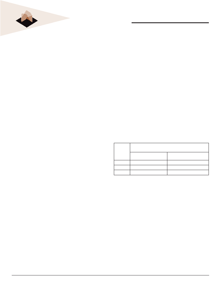
5
White Electronic Designs Corporation (602) 437-1520 www.whiteedc.com
White Electronic Designs
WEDPND16M72S-XBX
ALLOWABLE OPERATING
FREQUENCY (MHz)
CAS
SPEED
LATENCY = 2
LATENCY = 2.5
-200
75
100
-250
100
125
-266
100
133
selection of a burst length, a burst type, a CAS latency, and
an operating mode, as shown in Figure 3. The Mode Regis-
ter is programmed via the MODE REGISTER SET command
(with BA0 = 0 and BA1 = 0) and will retain the stored
information until it is programmed again or the device loses
power. (Except for bit A8 which is self clearing).
Reprogramming the mode register will not alter the contents
of the memory, provided it is performed correctly. The Mode
Register must be loaded (reloaded) when all banks are idle
and no bursts are in progress, and the controller must wait
the specified time before initiating the subsequent opera-
tion. Violating either of these requirements will result in un-
specified operation.
Mode register bits A0-A2 specify the burst length, A3 speci-
fies the type of burst (sequential or interleaved), A4-A6 specify
the CAS latency, and A7-A12 specify the operating mode.
Read and write accesses to the DDR SDRAM are burst ori-
ented, with the burst length being programmable, as shown
in Figure 3. The burst length determines the maximum num-
ber of column locations that can be accessed for a given
READ or WRITE command. Burst lengths of 2, 4 or 8 loca-
tions are available for both the sequential and the inter-
leaved burst types.
Reserved states should not be used, as unknown operation
or incompatibility with future versions may result.
When a READ or WRITE command is issued, a block of col-
umns equal to the burst length is effectively selected. All
accesses for that burst take place within this block, meaning
that the burst will wrap within the block if a boundary is
reached. The block is uniquely selected by A1-Ai when the
burst length is set to two; by A2-Ai when the burst length is
set to four (where Ai is the most significant column address
for a given configuration); and by A3-Ai when the burst
length is set to eight. The remaining (least significant) ad-
dress bit(s) is (are) used to select the starting location within
the block. The programmed burst length applies to both
READ and WRITE bursts.
BURST LENGTH
The READ latency is the delay, in clock cycles, between the
registration of a READ command and the availability of the first
bit of output data. The latency can be set to 2 or 2.5 clocks.
If a READ command is registered at clock edge
n, and the
latency is
m clocks, the data will be available by clock edge
n+m. Table 2 below indicates the operating frequencies at
which each CAS latency setting can be used.
Reserved states should not be used as unknown operation
or incompatibility with future versions may result.
BURST TYPE
Accesses within a given burst may be programmed to be
either sequential or interleaved; this is referred to as the
burst type and is selected via bit M3.
The ordering of accesses within a burst is determined by
the burst length, the burst type and the starting column
address, as shown in Table 1.
READ LATENCY
TABLE 2 - CAS LATENCY
OPERATING MODE
The normal operating mode is selected by issuing a MODE
REGISTER SET command with bits A7-A12 each set to zero,
and bits A0-A6 set to the desired values. A DLL reset is
initiated by issuing a MODE REGISTER SET command with
bits A7 and A9-A12 each set to zero, bit A8 set to one, and
bits A0-A6 set to the desired values. Although not required,
JEDEC specifications recommend when a LOAD MODE REG-
ISTER command is issued to reset the DLL, it should always
be followed by a LOAD MODE REGISTER command to se-
lect normal operating mode.
All other combinations of values for A7-A12 are reserved
for future use and/or test modes. Test modes and reserved
states should not be used because unknown operation or
incompatibility with future versions may result.
相关PDF资料 |
PDF描述 |
|---|---|
| WMS512K8-20FFIA | 512K X 8 STANDARD SRAM, 20 ns, DFP32 |
| WMS512K8-17FQA | 512K X 8 STANDARD SRAM, 17 ns, CDFP36 |
| WMS512K8-20CLQ | 512K X 8 STANDARD SRAM, 20 ns, CQCC32 |
| WMS512K8-45DEQA | 512K X 8 STANDARD SRAM, 45 ns, CDSO32 |
| WED3DG7266V10D1-SG | 64M X 72 SYNCHRONOUS DRAM MODULE, ZMA144 |
相关代理商/技术参数 |
参数描述 |
|---|---|
| WEDPNF8M721V-1010BC | 制造商:未知厂家 制造商全称:未知厂家 功能描述:8Mx72 Synchronous DRAM + 8Mb Flash Mixed Module Multi-Chip Package |
| WEDPNF8M721V-1010BI | 制造商:未知厂家 制造商全称:未知厂家 功能描述:8Mx72 Synchronous DRAM + 8Mb Flash Mixed Module Multi-Chip Package |
| WEDPNF8M721V-1010BM | 制造商:未知厂家 制造商全称:未知厂家 功能描述:8Mx72 Synchronous DRAM + 8Mb Flash Mixed Module Multi-Chip Package |
| WEDPNF8M721V-1012BC | 制造商:未知厂家 制造商全称:未知厂家 功能描述:8Mx72 Synchronous DRAM + 8Mb Flash Mixed Module Multi-Chip Package |
| WEDPNF8M721V-1012BI | 制造商:未知厂家 制造商全称:未知厂家 功能描述:8Mx72 Synchronous DRAM + 8Mb Flash Mixed Module Multi-Chip Package |
发布紧急采购,3分钟左右您将得到回复。