- 您现在的位置:买卖IC网 > PDF目录276857 > WEDPND16M72S-266BC (WHITE ELECTRONIC DESIGNS CORP) 16M X 72 DDR DRAM, 0.75 ns, PBGA219 PDF资料下载
参数资料
| 型号: | WEDPND16M72S-266BC |
| 厂商: | WHITE ELECTRONIC DESIGNS CORP |
| 元件分类: | DRAM |
| 英文描述: | 16M X 72 DDR DRAM, 0.75 ns, PBGA219 |
| 封装: | 32 X 25 MM, PLASTIC, BGA-219 |
| 文件页数: | 4/16页 |
| 文件大小: | 441K |
| 代理商: | WEDPND16M72S-266BC |
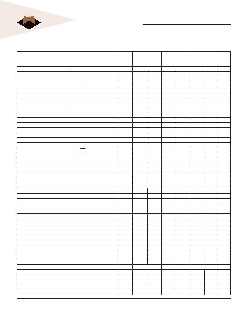
12
White Electronic Designs Corporation Phoenix AZ (602) 437-1520
White Electronic Designs
WEDPND16M72S-XBX
266 MHz CL 2.5
250 MHz CL2.5
200 MHz CL2.5
200 CL 2
200 MHz CL2
150 MHz CL2
Parameter
Symbol
Min
Max
Min
Max
Min
Max
Units
Access window of DQs from CLK/CLK
tAC
-0.75
+0.75
-0.8
+0.8
-0.8
+0.8
ns
CLK high-level width (30)
tCH
0.45
0.55
0.45
0.55
0.45
0.55
tCK
CLK low-level width (30)
tCL
0.45
0.55
0.45
0.55
0.45
0.55
tCK
Clock cycle time
CL = 2.5 (45, 52)
tCK (2.5)
7.5
13
8
13
10
13
ns
CL = 2 (45, 52)
tCK (2)
10
13
10
13
15
ns
DQ and DM input hold time relative to DQS (26, 31)
tDH
0.5
0.6
ns
DQ and DM input setup time relative to DQS (26, 31)
tDS
0.5
0.6
ns
DQ and DM input pulse width (for each input) (31)
tDIPW
1.75
2
ns
Access window of DQS from CLK/CLK
tDQSCK
-0.75
+0.75
-0.8
+0.8
-0.8
+0.8
ns
DQS input high pulse width
tDQSH
0.35
tCK
DQS input low pulse width
tDQSL
0.35
tCK
DQS-DQ skew, DQS to last DQ valid, per group, per access (25, 26)
tDQSQ
0.5
0.6
ns
Write command to first DQS latching transition
tDQSS
0.75
1.25
0.75
1.25
0.75
1.25
tCK
DQS falling edge to CLK rising - setup time
tDSS
0.2
tCK
DQS falling edge from CLK rising - hold time
tDSH
0.2
tCK
Half clock period (34)
tHP
tCH,tCL
ns
Data-out high-impedance window from CLK/CLK (18, 42)
tHZ
+0.75
+0.8
ns
Data-out low-impedance window from CLK/CLK (18, 43)
tLZ
-0.75
-0.8
ns
Address and control input hold time (fast slew rate) (14)
tIH
F
.90
1.1
ns
Address and control input setup time (fast slew rate) (14)
tIS
F
.90
1.1
ns
Address and control input hold time (slow slew rate) (14)
tIH
S
1
1.1
ns
Address and control input setup time (slow slew rate) (14)
tIS
S
1
1.1
ns
LOAD MODE REGISTER command cycle time
tMRD
15
16
ns
DQ-DQS hold, DQS to first DQ to go non-valid, per access (25, 26)
tQH
tHP-tQHS
ns
Data hold skew factor
tQHS
0.75
1
ns
ACTIVE to PRECHARGE command (35)
tRAS
40
120,000
40
120,000
40
120,000
ns
ACTIVE to READ with Auto precharge command (46)
tRAP
20
ns
ACTIVE to ACTIVE/AUTO REFRESH command period
tRC
65
70
ns
AUTO REFRESH command period (50)
tRFC
75
80
ns
ACTIVE to READ or WRITE delay
tRCD
20
ns
PRECHARGE command period
tRP
20
ns
DQS read preamble (42)
tRPRE
0.9
1.1
0.9
1.1
0.9
1.1
tCK
DQS read postamble
tRPST
0.4
0.6
0.4
0.6
0.4
0.6
tCK
ACTIVE bank a to ACTIVE bank b command
tRRD
15
ns
DQS write preamble
tWPRE
0.25
tCK
DQS write preamble setup time (20, 21)
tWPRES
00
0
ns
DQS write postamble (19)
tWPST
0.4
0.6
0.4
0.6
0.4
0.6
tCK
Write recovery time
tWR
15
ns
Internal WRITE to READ command delay
tWTR
11
1
tCK
Data valid output window (25)
na
tQH - tDQSQ
ns
REFRESH to REFRESH command interval (23)
tREFC
70.3
s
Average periodic refresh interval (23)
tREFI
7.8
s
Terminating voltage delay to VDD
tVTD
00
0
ns
Exit SELF REFRESH to non-READ command
tXSNR
75
80
ns
Exit SELF REFRESH to READ command
tXSRD
200
tCK
ELECTRICAL CHARACTERISTICS AND RECOMMENDED AC OPERATING CHARACTERISTICS
(NOTES 1-5, 14-17, 33)
相关PDF资料 |
PDF描述 |
|---|---|
| WMS512K8-20FFIA | 512K X 8 STANDARD SRAM, 20 ns, DFP32 |
| WMS512K8-17FQA | 512K X 8 STANDARD SRAM, 17 ns, CDFP36 |
| WMS512K8-20CLQ | 512K X 8 STANDARD SRAM, 20 ns, CQCC32 |
| WMS512K8-45DEQA | 512K X 8 STANDARD SRAM, 45 ns, CDSO32 |
| WED3DG7266V10D1-SG | 64M X 72 SYNCHRONOUS DRAM MODULE, ZMA144 |
相关代理商/技术参数 |
参数描述 |
|---|---|
| WEDPNF8M721V-1010BC | 制造商:未知厂家 制造商全称:未知厂家 功能描述:8Mx72 Synchronous DRAM + 8Mb Flash Mixed Module Multi-Chip Package |
| WEDPNF8M721V-1010BI | 制造商:未知厂家 制造商全称:未知厂家 功能描述:8Mx72 Synchronous DRAM + 8Mb Flash Mixed Module Multi-Chip Package |
| WEDPNF8M721V-1010BM | 制造商:未知厂家 制造商全称:未知厂家 功能描述:8Mx72 Synchronous DRAM + 8Mb Flash Mixed Module Multi-Chip Package |
| WEDPNF8M721V-1012BC | 制造商:未知厂家 制造商全称:未知厂家 功能描述:8Mx72 Synchronous DRAM + 8Mb Flash Mixed Module Multi-Chip Package |
| WEDPNF8M721V-1012BI | 制造商:未知厂家 制造商全称:未知厂家 功能描述:8Mx72 Synchronous DRAM + 8Mb Flash Mixed Module Multi-Chip Package |
发布紧急采购,3分钟左右您将得到回复。