- 您现在的位置:买卖IC网 > PDF目录276857 > WEDPND16M72S-266BC (WHITE ELECTRONIC DESIGNS CORP) 16M X 72 DDR DRAM, 0.75 ns, PBGA219 PDF资料下载
参数资料
| 型号: | WEDPND16M72S-266BC |
| 厂商: | WHITE ELECTRONIC DESIGNS CORP |
| 元件分类: | DRAM |
| 英文描述: | 16M X 72 DDR DRAM, 0.75 ns, PBGA219 |
| 封装: | 32 X 25 MM, PLASTIC, BGA-219 |
| 文件页数: | 13/16页 |
| 文件大小: | 441K |
| 代理商: | WEDPND16M72S-266BC |
6
White Electronic Designs Corporation Phoenix AZ (602) 437-1520
White Electronic Designs
WEDPND16M72S-XBX
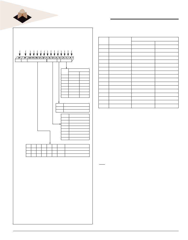
The extended mode register controls functions beyond
those controlled by the mode register; these additional
functions are DLL enable/disable, output drive strength, and
QFC. These functions are controlled via the bits shown in
Figure 5. The extended mode register is programmed via
the LOAD MODE REGISTER command to the mode register
(with BA0 = 1 and BA1 = 0) and will retain the stored
information until it is programmed again or the device loses
power. The enabling of the DLL should always be followed
by a LOAD MODE REGISTER command to the mode register
(BA0/BA1 both LOW) to reset the DLL.
The extended mode register must be loaded when all banks
are idle and no bursts are in progress, and the controller
must wait the specified time before initiating any subse-
quent operation. Violating either of these requirements
could result in unspecified operation.
EXTENDED MODE REGISTER
TABLE 1 - BURST DEFINITION
Burst Starting Column
Order of Accesses Within a Burst
Length
Address
A0
2
0
0-1
1
1-0
A1
A0
0
0-1-2-3
4
0
1
1-2-3-0
1-0-3-2
1
0
2-3-0-1
1
3-0-1-2
3-2-1-0
A2
A1
A0
0
0-1-2-3-4-5-6-7
0
1
1-2-3-4-5-6-7-0
1-0-3-2-5-4-7-6
0
1
0
2-3-4-5-6-7-0-1
2-3-0-1-6-7-4-5
8
0
1
3-4-5-6-7-0-1-2
3-2-1-0-7-6-5-4
1
0
4-5-6-7-0-1-2-3
1
0
1
5-6-7-0-1-2-3-4
5-4-7-6-1-0-3-2
1
0
6-7-0-1-2-3-4-5
6-7-4-5-2-3-0-1
1
7-0-1-2-3-4-5-6
7-6-5-4-3-2-1-0
Type = Sequential Type = Interleaved
NOTES:
1. For a burst length of two, A1-Ai select two-data-element block; A0 selects
the starting column within the block.
2. For a burst length of four, A2-Ai select four-data-element block; A0-1 select
the starting column within the block.
3. For a burst length of eight, A3-Ai select eight-data-element block; A0-2
select the starting column within the block.
4. Whenever a boundary of the block is reached within a given sequence
above, the following access wraps within the block.
FIG. 3 MODE REGISTER DEFINITION
M3 = 0
2
4
8
Reserved
M3 = 1
2
4
8
Reserved
Operating Mode
Normal Operation
Normal Operation/Reset DLL
All other states reserved
0
Valid
0
1
Burst Type
Sequential
Interleaved
CAS Latency
Reserved
2
Reserved
2.5
Reserved
Burst Length
M0
0
1
0
1
0
1
0
1
Burst Length
CAS Latency
BT
A9
A7
A6
A5
A4
A3
A8
A2
A1
A0
Mode Register (Mx)
Address Bus
M1
0
1
0
1
M2
0
1
M3
M4
0
1
0
1
0
1
0
1
M5
0
1
0
1
M6
0
1
M6-M0
M8
M7
Operating Mode
A10
A11
* M14 and M13
(BA0 and BA1 must be
"0, 0" to select
the base mode register
(vs. the extended
mode register).
0*
BA0
BA1
Reserved
M9
M10
M11
0
10
0
--
-
A12
M12
0
-
相关PDF资料 |
PDF描述 |
|---|---|
| WMS512K8-20FFIA | 512K X 8 STANDARD SRAM, 20 ns, DFP32 |
| WMS512K8-17FQA | 512K X 8 STANDARD SRAM, 17 ns, CDFP36 |
| WMS512K8-20CLQ | 512K X 8 STANDARD SRAM, 20 ns, CQCC32 |
| WMS512K8-45DEQA | 512K X 8 STANDARD SRAM, 45 ns, CDSO32 |
| WED3DG7266V10D1-SG | 64M X 72 SYNCHRONOUS DRAM MODULE, ZMA144 |
相关代理商/技术参数 |
参数描述 |
|---|---|
| WEDPNF8M721V-1010BC | 制造商:未知厂家 制造商全称:未知厂家 功能描述:8Mx72 Synchronous DRAM + 8Mb Flash Mixed Module Multi-Chip Package |
| WEDPNF8M721V-1010BI | 制造商:未知厂家 制造商全称:未知厂家 功能描述:8Mx72 Synchronous DRAM + 8Mb Flash Mixed Module Multi-Chip Package |
| WEDPNF8M721V-1010BM | 制造商:未知厂家 制造商全称:未知厂家 功能描述:8Mx72 Synchronous DRAM + 8Mb Flash Mixed Module Multi-Chip Package |
| WEDPNF8M721V-1012BC | 制造商:未知厂家 制造商全称:未知厂家 功能描述:8Mx72 Synchronous DRAM + 8Mb Flash Mixed Module Multi-Chip Package |
| WEDPNF8M721V-1012BI | 制造商:未知厂家 制造商全称:未知厂家 功能描述:8Mx72 Synchronous DRAM + 8Mb Flash Mixed Module Multi-Chip Package |
发布紧急采购,3分钟左右您将得到回复。