- 您现在的位置:买卖IC网 > PDF目录276857 > WEDPND16M72S-266BC (WHITE ELECTRONIC DESIGNS CORP) 16M X 72 DDR DRAM, 0.75 ns, PBGA219 PDF资料下载
参数资料
| 型号: | WEDPND16M72S-266BC |
| 厂商: | WHITE ELECTRONIC DESIGNS CORP |
| 元件分类: | DRAM |
| 英文描述: | 16M X 72 DDR DRAM, 0.75 ns, PBGA219 |
| 封装: | 32 X 25 MM, PLASTIC, BGA-219 |
| 文件页数: | 5/16页 |
| 文件大小: | 441K |
| 代理商: | WEDPND16M72S-266BC |
13
White Electronic Designs Corporation (602) 437-1520 www.whiteedc.com
White Electronic Designs
WEDPND16M72S-XBX
NOTES:
1. All voltages referenced to VSS.
2. Tests for AC timing, ICC, and electrical AC and DC characteristics may be
conducted at nominal reference/supply voltage levels, but the related
specifications and device operation are guaranteed for the full voltage
range specified.
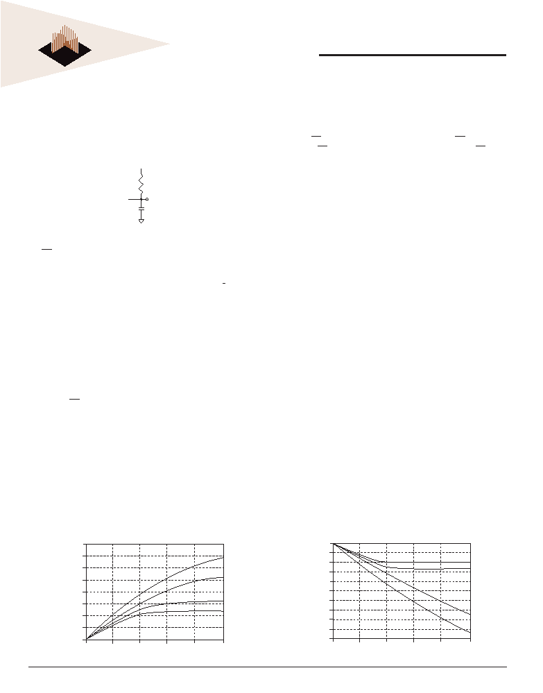
3. Outputs measured with equivalent load:
4. AC timing and ICC tests may use a VIL-to-VIH swing of up to 1.5V in the test
environment, but input timing is still referenced to VREF (or to the crossing point for
CLK/CLK), and parameter specifications are guaranteed for the specified AC input
levels under normal use conditions. The minimum slew rate for the input signals
used to test the device is 1V/ns in the range between VIL(AC) and VIH(AC).
5. The AC and DC input level specifications are as defined in the SSTL_2 Standard
(i.e., the receiver will effectively switch as a result of the signal crossing the AC
input level, and will remain in that state as long as the signal does not ring back
above [below] the DC input LOW [HIGH] level).
6. VREF is expected to equal VCCQ/2 of the transmitting device and to track
variations in the DC level of the same. Peak-to-peak noise (noncommon
mode) on VREF may not exceed ±2 percent of the DC value. Thus, from VCCQ/2,
VREF is allowed ±25mV for DC error and an additional ±25mV for AC noise. This
measurement is to be taken at the nearest VREF by-pass capacitor.
7. VTT is not applied directly to the device. VTT is a system supply for signal
termination resistors, is expected to be set equal to VREF and must track
variations in the DC level of VREF.
8. VID is the magnitude of the difference between the input level on CLK and the
input level on CLK.
9. The value of VIX and VMP are expected to equal VCCQ/2 of the transmitting
device and must track variations in the DC level of the same.
10. ICC is dependent on output loading and cycle rates. Specified values are
obtained with minimum cycle time with the outputs open.
11. Enables on-chip refresh and address counters.
12. ICC specifications are tested after the device is properly initialized, and is
averaged at the defined cycle rate.
13. This parameter is not tested but guaranteed by design. tA = 25°C, F = 1 MHz
14. Command/Address input slew rate = 0.5V/ns. For 266 MHz with slew rates
1V/ns and faster, tIS and tIH are reduced to 900ps. If the slew rate is less than 0.5V/
ns, timing must be derated: tIS has an additional 50ps per each 100mV/ns
reduction in slew rate from the 500mV/ns. tIH has 0ps added, that is, it remains
constant. If the slew rate exceeds 4.5V/ns, functionality is uncertain.
15. The CLK/CLK input reference level (for timing referenced to CLK/CLK) is the point at
which CLK and CLK cross; the input reference level for signals other than CLK/CLK is VREF.
16. Inputs are not recognized as valid until VREF stabilizes. Exception: during the
period before VREF stabilizes, CKE
0.3 x VCCQ is recognized as LOW.
17. The output timing reference level, as measured at the timing reference point
indicated in Note 3, is VTT.
18. tHZ and tLZ transitions occur in the same access time windows as valid data
transitions. These parameters are not referenced to a specific voltage level, but
specify when the device output is no longer driving (HZ) or begins driving (LZ).
19. The maximum limit for this parameter is not a device limit. The device will
operate with a greater value for this parameter, but system performance (bus
turnaround) will degrade accordingly.
20. This is not a device limit. The device will operate with a negative value, but
system performance could be degraded due to bus turnaround.
21. It is recommended that DQS be valid (HIGH or LOW) on or before the WRITE
command. The case shown (DQS going from High-Z to logic LOW) applies
when no WRITEs were previously in progress on the bus. If a previous WRITE was
in progress, DQS could be HIGH during this time, depending on tDQSS.
22. MIN (tRC or tRFC) for ICC measurements is the smallest multiple of tCK that meets
the minimum absolute value for the respective parameter. tRAS (MAX) for ICC
measurements is the largest multiple of tCK that meets the maximum absolute
value for tRAS.
23. The refresh period 64ms. This equates to an average refresh rate of 7.8125s.
However, an AUTO REFRESH command must be asserted at least once every
70.3s; burst refreshing or posting by the DRAM controller greater than eight
refresh cycles is not allowed.
24. The I/O capacitance per DQS and DQ byte/group will not differ by more
than this maximum amount for any given device.
25. The valid data window is derived by achieving other specifications - tHP
(tCK/2), tDQSQ, and tQH (tQH = tHP - tQHS). The data valid window derates directly
porportional with the clock duty cycle and a practical data valid window can
be derived. The clock is allowed a maximum duty cycle variation of 45/55.
Functionality is uncertain when operating beyond a 45/55 ratio. The data valid
window derating curves are provided below for duty cycles ranging between
50/50 and 45/55.
26. Referenced to each output group: LDQS with DQ0-DQ7; and UDQS with
DQ8-DQ15 of each chip.
27. This limit is actually a nominal value and does not result in a fail value. CKE is HIGH
during REFRESH command period (tRFC [MIN]) else CKE is LOW (i.e., during standby).
160
140
120
100
80
60
40
20
0
0.0
0.5
1.0
1.5
2.0
2.5
VOUT (V)
IOUT
(mA)
Maximum
Nominal high
Nominal low
Minimum
50
Reference
Point
30pF
Output
(VOUT)
VTT
FIG. A PULL-DOWN CHARACTERISTICS
FIG. B PULL-UP CHARACTERISTICS
0
-20
-40
-60
-80
-100
-120
-140
-160
-180
-200
0.0
0.5
1.0
1.5
2.0
2.5
VCCQ - VOUT (V)
IOUT
(mA)
Maximum
Nominal high
Nominal low
Minimum
相关PDF资料 |
PDF描述 |
|---|---|
| WMS512K8-20FFIA | 512K X 8 STANDARD SRAM, 20 ns, DFP32 |
| WMS512K8-17FQA | 512K X 8 STANDARD SRAM, 17 ns, CDFP36 |
| WMS512K8-20CLQ | 512K X 8 STANDARD SRAM, 20 ns, CQCC32 |
| WMS512K8-45DEQA | 512K X 8 STANDARD SRAM, 45 ns, CDSO32 |
| WED3DG7266V10D1-SG | 64M X 72 SYNCHRONOUS DRAM MODULE, ZMA144 |
相关代理商/技术参数 |
参数描述 |
|---|---|
| WEDPNF8M721V-1010BC | 制造商:未知厂家 制造商全称:未知厂家 功能描述:8Mx72 Synchronous DRAM + 8Mb Flash Mixed Module Multi-Chip Package |
| WEDPNF8M721V-1010BI | 制造商:未知厂家 制造商全称:未知厂家 功能描述:8Mx72 Synchronous DRAM + 8Mb Flash Mixed Module Multi-Chip Package |
| WEDPNF8M721V-1010BM | 制造商:未知厂家 制造商全称:未知厂家 功能描述:8Mx72 Synchronous DRAM + 8Mb Flash Mixed Module Multi-Chip Package |
| WEDPNF8M721V-1012BC | 制造商:未知厂家 制造商全称:未知厂家 功能描述:8Mx72 Synchronous DRAM + 8Mb Flash Mixed Module Multi-Chip Package |
| WEDPNF8M721V-1012BI | 制造商:未知厂家 制造商全称:未知厂家 功能描述:8Mx72 Synchronous DRAM + 8Mb Flash Mixed Module Multi-Chip Package |
发布紧急采购,3分钟左右您将得到回复。