- 您现在的位置:买卖IC网 > PDF目录297791 > WLA49VVA (National Semiconductor Corporation) Audio Sub-System with Dual-Mode Stereo Headphone and Mono High Efficiency Loudspeaker Amplifiers and Multi-Purpose ADC PDF资料下载
参数资料
| 型号: | WLA49VVA |
| 厂商: | National Semiconductor Corporation |
| 元件分类: | ADC |
| 英文描述: | Audio Sub-System with Dual-Mode Stereo Headphone and Mono High Efficiency Loudspeaker Amplifiers and Multi-Purpose ADC |
| 中文描述: | 音频子系统的双模单声道立体声耳机和扬声器放大器的高效率和多功能模数转换器 |
| 文件页数: | 21/112页 |
| 文件大小: | 5017K |
| 代理商: | WLA49VVA |
第1页第2页第3页第4页第5页第6页第7页第8页第9页第10页第11页第12页第13页第14页第15页第16页第17页第18页第19页第20页当前第21页第22页第23页第24页第25页第26页第27页第28页第29页第30页第31页第32页第33页第34页第35页第36页第37页第38页第39页第40页第41页第42页第43页第44页第45页第46页第47页第48页第49页第50页第51页第52页第53页第54页第55页第56页第57页第58页第59页第60页第61页第62页第63页第64页第65页第66页第67页第68页第69页第70页第71页第72页第73页第74页第75页第76页第77页第78页第79页第80页第81页第82页第83页第84页第85页第86页第87页第88页第89页第90页第91页第92页第93页第94页第95页第96页第97页第98页第99页第100页第101页第102页第103页第104页第105页第106页第107页第108页第109页第110页第111页第112页
11.0 System Control
Method 1. I
2C Compatible Interface
11.1 I
2C SIGNALS
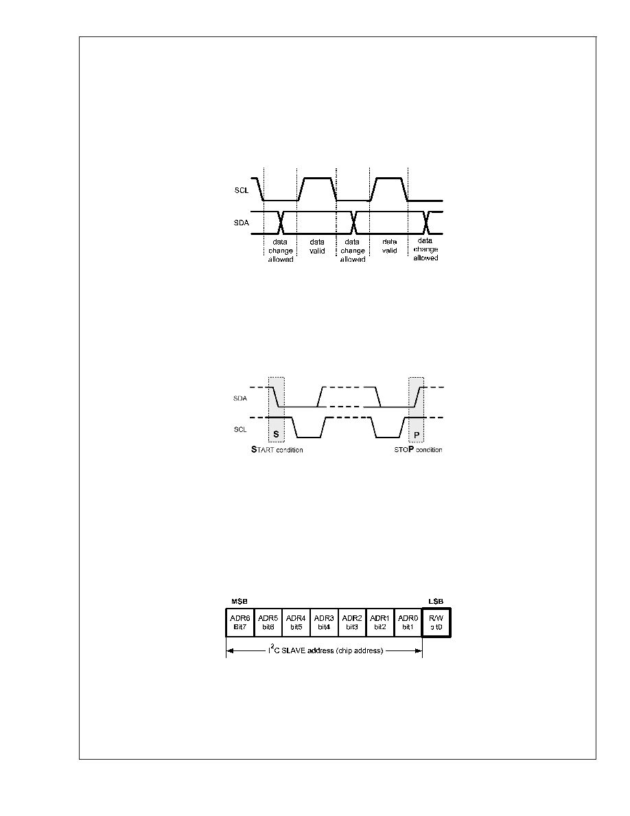
In I
2C mode the LM4935 pin SCL is used for the I2C clock SCL and the pin SDA is used for the I2C data signal SDA. Both these
signals need a pull-up resistor according to I
2C specification. The I2C slave address for LM4935 is 0011010
2.
11.2 I
2C DATA VALIDITY
The data on SDA line must be stable during the HIGH period of the clock signal (SCL). In other words, state of the data line can
only be changed when SCL is LOW.
201341Q1
I
2C Signals: Data Validity
11.3 I
2C START AND STOP CONDITIONS
START and STOP bits classify the beginning and the end of the I
2C session. START condition is defined as SDA signal
transitioning from HIGH to LOW while SCL line is HIGH. STOP condition is defined as the SDA transitioning from LOW to HIGH
while SCL is HIGH. The I
2C master always generates START and STOP bits. The I2C bus is considered to be busy after START
condition and free after STOP condition. During data transmission, I
2C master can generate repeated START conditions. First
START and repeated START conditions are equivalent, function-wise.
201341Q2
11.4 TRANSFERRING DATA
Every byte put on the SDA line must be eight bits long, with the most significant bit (MSB) being transferred first. Each byte of data
has to be followed by an acknowledge bit. The acknowledge related clock pulse is generated by the master. The transmitter
releases the SDA line (HIGH) during the acknowledge clock pulse. The receiver must pull down the SDA line during the 9
th clock
pulse, signifying an acknowledge. A receiver which has been addressed must generate an acknowledge after each byte has been
received.
After the START condition, the I
2C master sends a chip address. This address is seven bits long followed by an eighth bit which
is a data direction bit (R/W). The LM4935 address is 0011010
2. For the eighth bit, a “0” indicates a WRITE and a “1” indicates a
READ. The second byte selects the register to which the data will be written. The third byte contains data to write to the selected
register.
201341Q3
I
2C Chip Address
Register changes take an effect at the SCL rising edge during the last ACK from slave.
LM4935
www.national.com
16
相关PDF资料 |
PDF描述 |
|---|---|
| WMS512K8-55CI | 512Kx8 MONOLITHIC SRAM |
| WMS512K8-55CIA | 512Kx8 MONOLITHIC SRAM |
| WMS512K8-55CLC | 512Kx8 MONOLITHIC SRAM |
| WMS512K8-55CLI | 512Kx8 MONOLITHIC SRAM |
| WMS512K8-55CLIA | 512Kx8 MONOLITHIC SRAM |
相关代理商/技术参数 |
参数描述 |
|---|---|
| WL-A-7079B-12 | 制造商:WAMCO 功能描述:12V 40W AV REFL GG12A BAY15S 制造商:WAMCO 功能描述:12V 40W AV REFL GG12A BAY15s |
| WL-A-7079B-24 | 制造商:WAMCO 功能描述:28V 40W AV REFL GG12A BAY15S |
| WL-A-7512-12 | 制造商:WAMCO 功能描述:14V 26W AV REFL GG10 BAY15S |
| WL-A-7512-24 | 制造商:WAMCO 功能描述:28V 26W AV REFL GG10 BAY15S |
| WL-A-7796A-24 | 制造商:WAMCO 功能描述:28V 14W/40W AV REFL GG12A BAY15D DUAL FILAMENT |
发布紧急采购,3分钟左右您将得到回复。