参数资料
| 型号: | X45620V20I-2.7 |
| 厂商: | Intersil |
| 文件页数: | 14/20页 |
| 文件大小: | 0K |
| 描述: | IC VOLT MON DUAL SW EEPR 20TSSOP |
| 标准包装: | 75 |
| 类型: | 多压监控器 |
| 监视电压数目: | 2 |
| 输出: | 开路漏极或开路集电极 |
| 复位: | 低有效 |
| 复位超时: | 最小为 75 ms |
| 电压 - 阀值: | 1.75V,2.62V |
| 工作温度: | -40°C ~ 85°C |
| 安装类型: | 表面贴装 |
| 封装/外壳: | 20-TSSOP(0.173",4.40mm 宽) |
| 供应商设备封装: | 20-TSSOP |
| 包装: | 管件 |
�� �
�
�X45620�
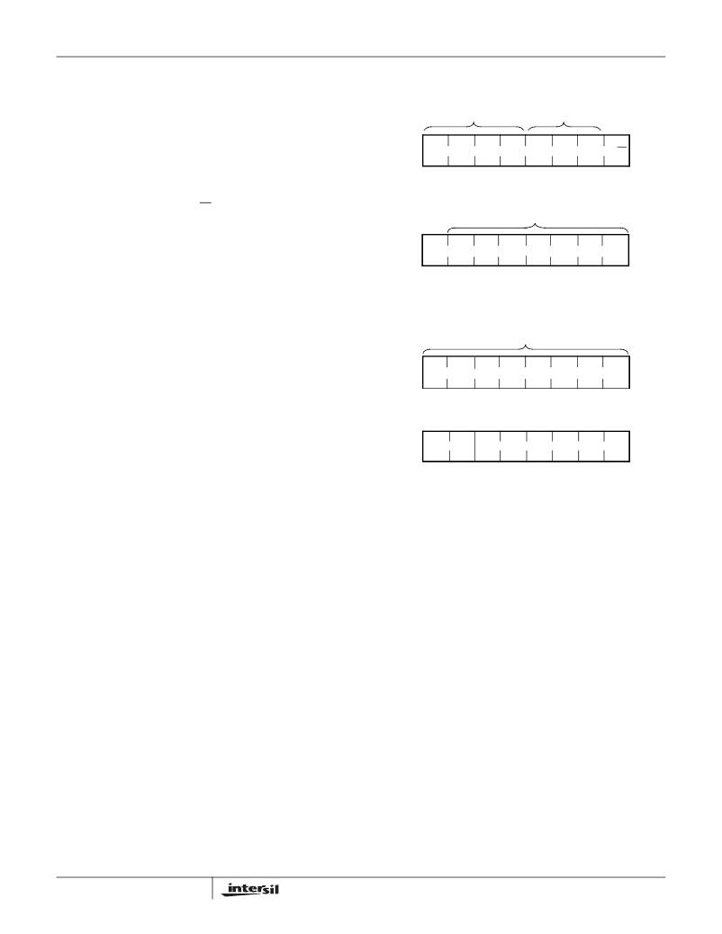
�DEVICE� ADDRESSING�
�Figure� 10.� Device� Addressing�
�Following� a� start� condition,� the� master� must� output� the�
�address� of� the� slave� it� is� accessing.� The� first� four� bits�
�of� the� Slave� Address� Byte� are� the� device� type� identi-�
�fier� bits.� These� must� equal� “1010”.� The� next� 3� bits� are�
�Device� Type�
�Identifier�
�Device�
�Select�
�the� device� select� bits� “0”,� S� 1� ,� and� S� 0� .� This� allows� up� to�
�1�
�0�
�1�
�0�
�0�
�S� 1�
�S� 0�
�R/W�
�4� devices� to� share� a� single� bus.� These� bits� are� com-�
�pared� to� the� S� 0� ,� S� 1� ,� device� select� input� pins.� The� last�
�bit� of� the� Slave� Address� Byte� defines� the� operation� to�
�be� performed.� When� the� R/W� bit� is� a� one,� then� a� read�
�operation� is� selected.� When� it� is� zero� then� a� write�
�operation� is� selected.� Refer� to� Figure� 10.� After� loading�
�Slave� Address� Byte�
�High� Order� Word� Address�
�the� Slave� Address� Byte� from� the� SDA� bus,� the� device�
�*�
�A14� A13� A12�
�A11� A10�
�A9�
�A8�
�compares� the� device� type� bits� with� the� value� “1010”�
�and� the� device� select� bits� with� the� status� of� the� device�
�select� input� pins.� If� the� compare� is� not� successful,� no�
�acknowledge� is� output� during� the� ninth� clock� cycle� and�
�the� device� returns� to� the� standby� mode.�
�On� power-up� the� internal� address� is� undefined,� so� the�
�first� read� or� write� operation� must� supply� an� address.�
�X45620� Word� Address� Byte� 1�
�*This� bit� is� 0� for� access� to� the� array� and�
�1� for� access� to� the� Control� Register�
�Low� Order� Word� Address�
�The� word� address� is� either� supplied� by� the� master� or�
�A7�
�A6�
�A5�
�A4�
�A3�
�A2�
�A1�
�A0�
�obtained� from� an� internal� counter,� depending� on� the�
�operation.� The� master� must� supply� the� initial� two� Word�
�Address� Bytes� as� shown� in� Figure� 10.�
�Word� Address� Byte� 0�
�The� internal� organization� of� the� E� 2� array� is� 512� pages�
�D7�
�D6�
�D5�
�D4�
�D3�
�D2�
�D1�
�D0�
�by� 64� bytes� per� page.� The� page� address� is� partially�
�contained� in� the� Word� Address� Byte� 1� and� partially� in�
�bits� 7� through� 6� of� the� Word� Address� Byte� 0.� The� byte�
�address� is� contained� in� bits� 5� through� 0� of� the� Word�
�Address� Byte� 0.� See� Figure� 10.�
�WRITE� OPERATIONS�
�Byte� Write�
�For� a� write� operation,� the� device� follows� “3� byte”� proto-�
�col,� consisting� of� one� Slave� Address� Byte,� one� Word�
�Address� Byte� 1,� and� the� Word� Address� Byte� 0,� which�
�gives� the� master� access� to� any� one� of� the� words� in� the�
�array.� Upon� receipt� of� the� Word� Address� Byte� 0,� the�
�device� responds� with� an� acknowledge,� and� waits� for�
�the� first� eight� bits� of� data.� After� receiving� the� 8� bits� of�
�the� data� byte,� the� device� again� responds� with� an�
�acknowledge.� The� master� then� terminates� the� transfer�
�by� generating� a� stop� condition,� at� which� time� the�
�device� begins� the� internal� write� cycle� to� the� nonvolatile�
�memory.� While� the� internal� write� cycle� is� in� progress�
�the� device� inputs� are� disabled� and� the� device� will� not�
�respond� to� any� requests� from� the� master.� The� SDA� pin�
�is� at� high� impedance.� See� Figure� 11.� Refer� to� bus� tim-�
�ing� on� page� 21.�
�14�
�Data� Byte�
�Page� Write�
�The� device� is� capable� of� a� 64� byte� page� write� operation.�
�It� is� initiated� in� the� same� manner� as� the� byte� write�
�operation;� but� instead� of� terminating� the� write� operation�
�after� the� first� data� word� is� transferred,� the� master� can�
�transmit� up� to� sixty-three� more� words.� The� device� will�
�respond� with� an� acknowledge� after� the� receipt� of� each�
�word,� and� then� the� byte� address� is� internally� incre-�
�mented� by� one.� The� page� address� remains� constant.�
�When� the� counter� reaches� the� end� of� the� page,� it� “rolls�
�over”� and� goes� back� to� the� first� byte� of� the� current�
�page.� This� means� that� the� master� can� write� 64-bytes�
�to� the� page� beginning� at� any� byte.� If� the� master� begins�
�writing� at� byte� 32,� and� loads� 64-bytes,� then� the� first�
�32-bytes� are� written� to� bytes� 32� through� 63,� and� the�
�last� 16� words� are� written� to� bytes� 0� through� 31.� After-�
�wards,� the� address� counter� would� point� to� byte� 32.� If�
�the� master� writes� more� than� 64� bytes,� then� the� previ-�
�ously� loaded� data� is� overwritten� by� the� new� data,� one�
�byte� at� a� time.�
�FN8250.0�
�July� 29,� 2005�
�相关PDF资料 |
PDF描述 |
|---|---|
| X4645V8I-4.5A | IC SUPERVISOR CPU 64K EE 8-TSSOP |
| X4C105V20I | IC SUPERVISOR NOVRAM/EE 20-TSSOP |
| X5001V8I-4.5A | IC SUPERVISOR CPU 8-TSSOP |
| X5045V14I-4.5A | IC SUPERVISOR CPU 4K EE 14-TSSOP |
| X5083V8I-4.5A | IC SUPERVISOR CPU 8K EE 8-TSSOP |
相关代理商/技术参数 |
参数描述 |
|---|---|
| X45BS4H47 | 制造商:n/a 功能描述:Power SCR |
| X45C613 | 制造商:Rochester Electronics LLC 功能描述:- Bulk 制造商:Harris Corporation 功能描述: |
| X45C661 | 制造商:Harris Corporation 功能描述: |
| X45E333 | 制造商:Rochester Electronics LLC 功能描述:- Bulk 制造商:Harris Corporation 功能描述: |
| X45E333E | 制造商:Harris Corporation 功能描述: |
发布紧急采购,3分钟左右您将得到回复。