参数资料
| 型号: | X45620V20I-2.7 |
| 厂商: | Intersil |
| 文件页数: | 17/20页 |
| 文件大小: | 0K |
| 描述: | IC VOLT MON DUAL SW EEPR 20TSSOP |
| 标准包装: | 75 |
| 类型: | 多压监控器 |
| 监视电压数目: | 2 |
| 输出: | 开路漏极或开路集电极 |
| 复位: | 低有效 |
| 复位超时: | 最小为 75 ms |
| 电压 - 阀值: | 1.75V,2.62V |
| 工作温度: | -40°C ~ 85°C |
| 安装类型: | 表面贴装 |
| 封装/外壳: | 20-TSSOP(0.173",4.40mm 宽) |
| 供应商设备封装: | 20-TSSOP |
| 包装: | 管件 |
�� �
�
�X45620�
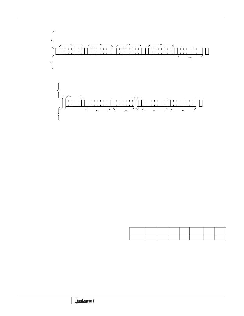
�Figure� 15.� Random� Read� Sequence�
�S�
�S�
�Signals� from�
�the� Master�
�T�
�A�
�R�
�Slave�
�Address�
�Word� Address�
�Byte� 1�
�Word� Address�
�Byte� 0�
�T�
�A�
�R�
�Slave�
�Address�
�S�
�T�
�O�
�T�
�T�
�P�
�SDA� Bus�
�S� 1� 0� 1� 0� 0� S� 1� S� 0� 0�
�S�
�1�
�P�
�Signals� from�
�the� Slave�
�A�
�C�
�K�
�A�
�C�
�K�
�A�
�C�
�K�
�A�
�C�
�K�
�Data�
�Figure� 16.� Sequential� Read� Sequence�
�Signals� from�
�the� Master�
�SDA� Bus�
�Slave�
�Address�
�S� 1� S� 0� 1�
�S�
�A�
�C�
�K�
�A�
�C�
�K�
�A�
�C�
�K�
�S�
�T�
�O�
�P�
�P�
�A�
�Signals� from�
�the� Slave�
�C�
�K�
�Data�
�(1)�
�Data�
�(2)�
�Data�
�(n–1)�
�Data�
�(n)�
�(n� is� any� integer� greater� than� 1)�
�Sequential� Read�
�Sequential� reads� can� be� initiated� as� either� a� current�
�address� read� or� random� read.� The� first� Data� Byte� is�
�transmitted� as� with� the� other� modes;� however,� the�
�master� now� responds� with� an� acknowledge,� indicating�
�it� requires� additional� data.� The� device� continues� to�
�output� data� for� each� acknowledge� received.� The� master�
�terminates� the� read� operation� by� not� responding� with� an�
�acknowledge� and� then� issuing� a� stop� condition.�
�The� data� output� is� sequential,� with� the� data� from�
�address� n� followed� by� the� data� from� address� n� +� 1.�
�The� address� counter� for� read� operations� increments�
�through� all� byte� addresses,� allowing� the� entire� memory�
�contents� to� be� read� during� one� operation.� At� the� end� of�
�the� address� space� the� counter� “rolls� over”� to� address�
�0000h� and� the� device� continues� to� output� data� for�
�each� acknowledge� received.� Refer� to� Figure� 16� for� the�
�acknowledge� and� data� transfer� sequence.�
�CONTROL� REGISTER� (CR)�
�The� user� must� issue� a� stop,� after� sending� this� byte� to�
�the� register,� to� initiate� the� high� voltage� cycle� that�
�writes� PUP,� WD1,� WD0,� BP1,� BP0� and� WPEN� to� the�
�nonvolatile� bits.� The� part� will� not� acknowledge� any�
�data� bytes� written� after� the� first� byte� is� entered.� A� stop�
�must� also� be� issued� after� a� volatile� register� write� oper-�
�ation� to� put� the� device� into� Standby.� After� a� write� to� the�
�CR,� the� address� counter� contents� are� undefined.�
�The� state� of� the� CR� can� be� read� by� performing� a� ran-�
�dom� read� at� the� address� of� the� register� at� any� time.�
�Only� one� byte� is� read� by� the� register� read� operation.�
�The� part� will� reset� itself� after� the� first� byte� is� read.� The�
�master� should� supply� a� stop� condition� to� be� consistent�
�with� the� bus� protocol,� but� a� stop� is� not� required� to� end�
�this� operation.� After� the� read� of� the� CR,� the� address�
�counter� contents� are� reset� to� zero,� but� the� user� will� be�
�told� these� bits� are� undefined� and� instructed� to� do� a�
�random� read.�
�Table� 1.� Control� Register�
�The� Control� Register� is� located� in� an� area� logically�
�7�
�6�
�5�
�4�
�3�
�2�
�1�
�0�
�separated� from� the� array� and� is� only� accessible� via� a�
�byte� write� to� the� register� address� of� FFFFH.� The� Con-�
�WPEN� WD1�
�WD0� BP1� BP0� RWEL� WEL� PUP�
�trol� Register� is� physically� part� of� the� array.�
�The� CR� can� only� be� modified� by� performing� a� byte� write�
�operation� directly� to� the� address� of� the� register� and� only�
�one� data� byte� is� allowed� for� each� register� write� operation.�
�Prior� to� initiating� a� nonvolatile� write� to� the� CR,� the� WEL�
�and� RWEL� bits� must� be� set� using� a� two� step� process,�
�with� the� whole� sequence� requiring� 3� steps.�
�17�
�RWEL:� Register� Write� Enable� Latch� (Volatile)�
�The� RWEL� bit� must� be� set� to� “1”� prior� to� a� write� to�
�Control� Register.�
�FN8250.0�
�July� 29,� 2005�
�相关PDF资料 |
PDF描述 |
|---|---|
| X4645V8I-4.5A | IC SUPERVISOR CPU 64K EE 8-TSSOP |
| X4C105V20I | IC SUPERVISOR NOVRAM/EE 20-TSSOP |
| X5001V8I-4.5A | IC SUPERVISOR CPU 8-TSSOP |
| X5045V14I-4.5A | IC SUPERVISOR CPU 4K EE 14-TSSOP |
| X5083V8I-4.5A | IC SUPERVISOR CPU 8K EE 8-TSSOP |
相关代理商/技术参数 |
参数描述 |
|---|---|
| X45BS4H47 | 制造商:n/a 功能描述:Power SCR |
| X45C613 | 制造商:Rochester Electronics LLC 功能描述:- Bulk 制造商:Harris Corporation 功能描述: |
| X45C661 | 制造商:Harris Corporation 功能描述: |
| X45E333 | 制造商:Rochester Electronics LLC 功能描述:- Bulk 制造商:Harris Corporation 功能描述: |
| X45E333E | 制造商:Harris Corporation 功能描述: |
发布紧急采购,3分钟左右您将得到回复。