参数资料
| 型号: | X96012V14IZT1 |
| 厂商: | Intersil |
| 文件页数: | 11/23页 |
| 文件大小: | 0K |
| 描述: | IC BIAS CTRLR UNIV SNSR 14-TSSOP |
| 标准包装: | 2,500 |
| 类型: | 传感器调节器 |
| 输入类型: | 电压 |
| 输出类型: | 电压 |
| 接口: | 2 线 |
| 电流 - 电源: | 15mA |
| 安装类型: | 表面贴装 |
| 封装/外壳: | 14-TSSOP(0.173",4.40mm 宽) |
| 供应商设备封装: | 14-TSSOP |
| 包装: | 带卷 (TR) |
19
FN8216.3
February 20, 2008
Slave Address Byte
Following a START condition, the master must output a
Slave Address Byte. Refer to Figure 16. This byte includes
three parts:
The four MSBs (SA7 - SA4) are the Device Type
Identifier, which must always be set to 1010 in order to
select the X96012.
The next three bits (SA3 - SA1) are the Device Address bits
(AS2 - AS0). To access any part of the X96012’s memory,
the value of bits AS2, AS1, and AS0 must correspond to the
logic levels at pins A2, A1, and A0 respectively.
The LSB (SA0) is the R/W bit. This bit defines the operation
to be performed on the device being addressed. When the
R/W bit is “1”, then a Read operation is selected. A “0”
selects a Write operation (refer to Figure 16).
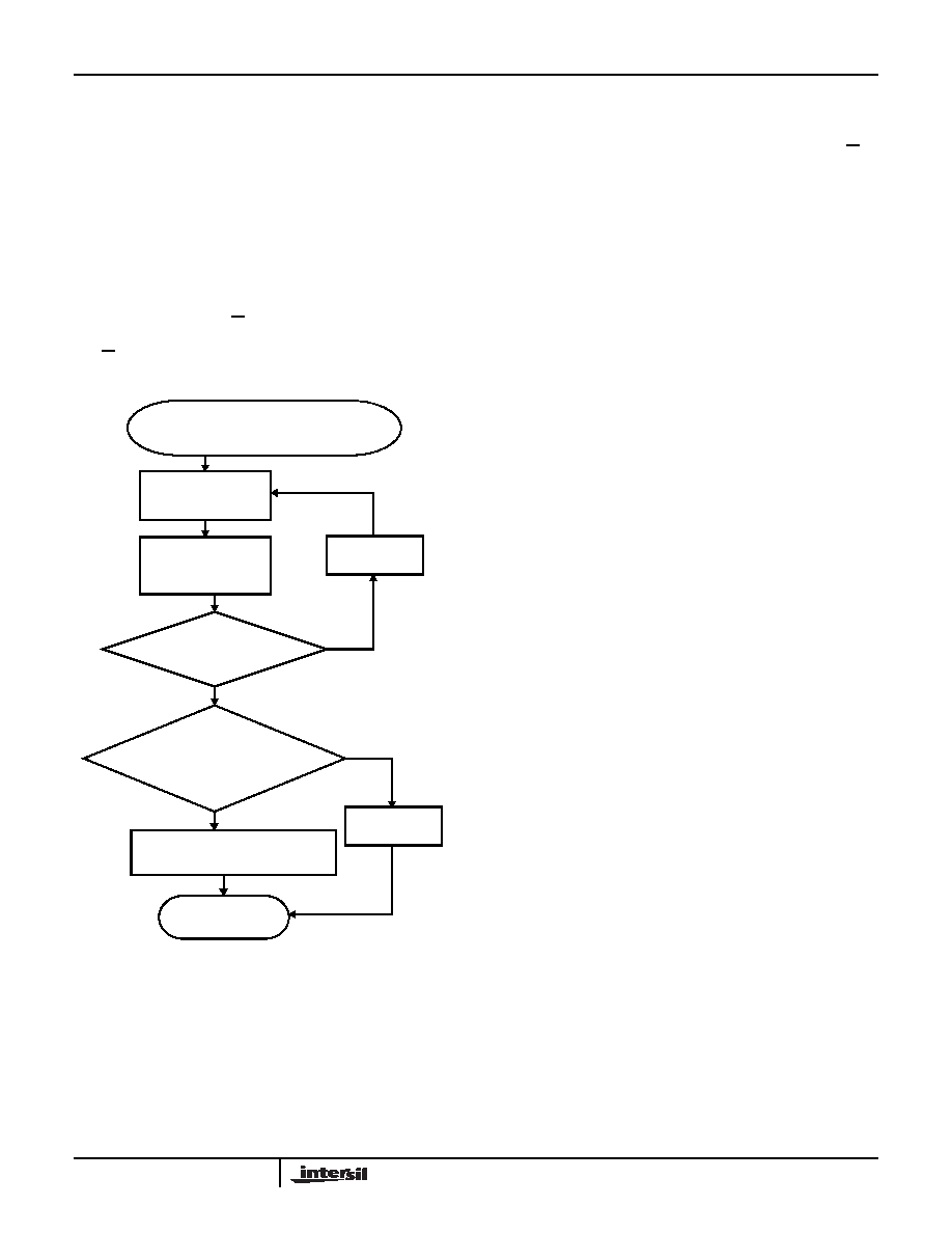
Nonvolatile Write Acknowledge Polling
After a nonvolatile write command sequence is correctly
issued (including the final STOP condition), the X96012
initiates an internal high voltage write cycle. This cycle
typically requires 5ms. During this time, any Read or Write
command is ignored by the X96012. Write Acknowledge
Polling is used to determine whether a high voltage write
cycle is completed.
During acknowledge polling, the master first issues a START
condition followed by a Slave Address Byte. The Slave
Address Byte contains the X96012’s Device Type Identifier
and Device Address. The LSB of the Slave Address (R/W)
can be set to either 1 or 0 in this case. If the device is busy
within the high voltage cycle, then no ACK is returned. If the
high voltage cycle is completed, an ACK is returned and the
master can then proceed with a new Read or Write
operation. Refer to Figure 17.
Byte Write Operation
In order to perform a Byte Write operation to the memory
array, the Write Enable Latch (WEL) bit of the Control 6
Register must first be set to “1”. See “WEL: Write Enable
For any Byte Write operation, the X96012 requires the Slave
Address Byte, an Address Byte, and a Data Byte. See
Figure 18. After each of them, the X96012 responds with an
ACK. The master then terminates the transfer by generating a
STOP condition. At this time, if all data bits are volatile, the
X96012 is ready for the next read or write operation. If some
bits are nonvolatile, the X96012 begins the internal write cycle
to the nonvolatile memory. During the internal nonvolatile write
cycle, the X96012 does not respond to any requests from the
master. The SDA output is at high impedance.
A Byte Write operation can access bytes at locations 00h
through FEh directly, when setting the Address Byte to 00h
through FEh respectively. Setting the Address Byte to FFh
accesses the byte at location 100h. The other sixteen bytes,
at locations FFh and 101h through 10Fh can only be
accessed using Page Write operations. The byte at location
FFh can only be written using a “Page Write” operation.
Writing to Control bytes which are located at byte addresses
80h through 8Fh is a special case described in “Writing to
Page Write Operation
The 2176-bit memory array is physically realized as one
contiguous array, organized as 17 pages of 16 bytes each. A
“Page Write” operation can be performed to any of the GPM
or LUT pages. In order to perform a Page Write operation to
the memory array, the Write Enable Latch (WEL) bit in
Control register 6 must first be set See “WEL: Write Enable
A Page Write operation is initiated in the same manner as
the byte write operation; but instead of terminating the write
cycle after the first data byte is transferred, the master can
transmit up to 16 bytes (see Figure 19). After the receipt of
each byte, the X96012 responds with an ACK, and the
internal byte address counter is incremented by one. The
page address remains constant. When the counter reaches
the end of the page, it “rolls over” and goes back to the first
byte of the same page.
ACK RETURNED?
ISSUE SLAVE
ADDRESS BYTE
(READ OR WRITE)
BYTE LOAD COMPLETED BY ISSUING
STOP. ENTER ACK POLLING
ISSUE STOP
ISSUE START
NO
YES
NO
CONTINUE NORMAL READ OR
WRITE COMMAND SEQUENCE
PROCEED
YES
COMPLETE. CONTINUE COMMAND
SEQUENCE.
HIGH VOLTAGE
ISSUE STOP
FIGURE 17. ACKNOWLEDGE POLLING SEQUENCE
X96012
相关PDF资料 |
PDF描述 |
|---|---|
| X9C303V8T2 | IC XDCP 100-TAP 32K EE 8-TSSOP |
| X9C503ST2 | IC XDCP 100-TAP 50K EE 8-SOIC |
| XA2C128-8CPG132Q | IC CPLD 128MC 100 I/O 132CSBGA |
| XA2C32A-7VQG44Q | IC CPLD 32MCELL 33 I/O 44-VQFP |
| XA2C384-11TQG144Q | IC CPLD 384MCELL 118 I/O 144TQFP |
相关代理商/技术参数 |
参数描述 |
|---|---|
| X9601XEVAL | 制造商:Intersil Corporation 功能描述:X9601 EVALUATION BOARD - Bulk |
| X9650M | 制造商:EPCOS 制造商全称:EPCOS 功能描述:Bandpass Filter |
| X-97-488 | 制造商:Brady Corporation 功能描述:Labels External Width:0.9" 制造商:Brady Corporation 功能描述:LABEL IDENTIFICATION 22.86X22.86 BLK/WHT; Background Color:White; Color:Black on White; External Width:0.9"; For Use With:IDXPERT Hand-Held Labeler; Label Material:Polyester; Label Size:22.86 x 22.86mm; Label Type:Identification ;RoHS Compliant: Yes |
| X97494 | 制造商:Mersen 功能描述:FUSE BS88-4 25A |
| X98014 | 制造商:INTERSIL 制造商全称:Intersil Corporation 功能描述:140MHz Triple Video Digitizer with Digital PLL |
发布紧急采购,3分钟左右您将得到回复。