参数资料
| 型号: | X96012V14IZT1 |
| 厂商: | Intersil |
| 文件页数: | 12/23页 |
| 文件大小: | 0K |
| 描述: | IC BIAS CTRLR UNIV SNSR 14-TSSOP |
| 标准包装: | 2,500 |
| 类型: | 传感器调节器 |
| 输入类型: | 电压 |
| 输出类型: | 电压 |
| 接口: | 2 线 |
| 电流 - 电源: | 15mA |
| 安装类型: | 表面贴装 |
| 封装/外壳: | 14-TSSOP(0.173",4.40mm 宽) |
| 供应商设备封装: | 14-TSSOP |
| 包装: | 带卷 (TR) |
2
FN8216.3
February 20, 2008
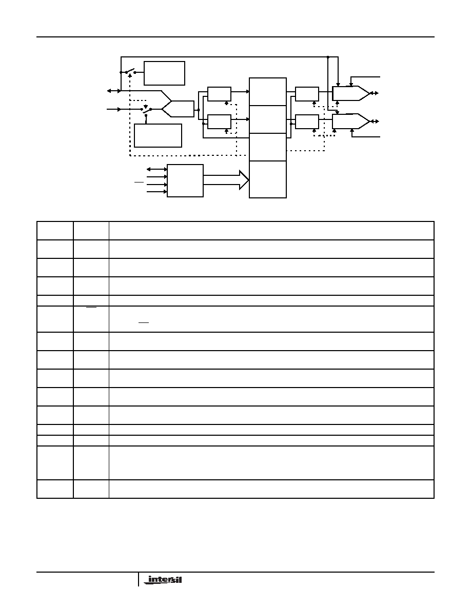
Block Diagram
Pin Descriptions
SDA
SCL
WP
2-WIRE
I2
VREF
R2
VSENSE
INTERFACE
A2, A1, A0
DAC 2
ADC
LOOK-UP
TABLE 1
LOOK-UP
TABLE 2
CONTROL
AND STATUS
GENERAL
PURPOSE
MEMORY
MUX
I1
R1
DAC 1
MUX
TEMPERATURE
SENSOR
VOLTAGE
REFERENCE
PIN
NUMBER
PIN
NAME
PIN DESCRIPTION
1A0
Device Address Select Pin 0. This pin determines the LSB of the device address required to communicate using the
2-wire interface. The A0 pin has an on-chip pull-down resistor.
2A1
Device Address Select Pin 1. This pin determines the intermediate bit of the device address required to communicate
using the 2-wire interface. The A1 pin has an on-chip pull-down resistor.
3A2
Device Address Select Pin 2. This pin determines the MSB of the device address required to communicate using the
2-wire interface. The A2 pin has an on-chip pull-down resistor.
4VCC
Supply Voltage.
5WP
Write Protect Control Pin. This pin is a CMOS compatible input. When LOW, Write Protection is enabled preventing
any “Write” operation. When HIGH, various areas of the memory can be protected using the Block Lock bits BL1 and
BL0. The WP pin has an on-chip pull-down resistor, which enables the Write Protection when this pin is left floating.
6SCL
Serial Clock. This is a TTL compatible input pin. This input is the 2-wire interface clock controlling data input and output
at the SDA pin.
7SDA
Serial Data. This pin is the 2-wire interface data into or out of the device. It is TTL compatible when used as an input,
and it is Open Drain when used as an output. This pin requires an external pull-up resistor.
8I1
Current Generator 1 Output. This pin sinks or sources current. The magnitude and direction of the current is fully
programmable and adaptive. The resolution is 8 bits.
9R1
Current Programming Resistor 1. A resistor between this pin and V
SS can set the maximum output current available
at pin I1. If no resistor is used, the maximum current must be selected using control register bits.
10
R2
Current Programming Resistor 2. A resistor between this pin and VSS can set the maximum output current available
at pin I2. If no resistor is used, the maximum current must be selected using control register bits.
11
VSS
Ground.
12
VSENSE
Sensor Voltage Input. This voltage input may be used to drive the input of the on-chip A/D converter.
13
VREF
Reference Voltage Input or Output. This pin can be configured as either an Input or an Output. As an Input, the
voltage at this pin is provided by an external source. As an Output, the voltage at this pin is a buffered output voltage
of the on-chip bandgap reference circuit. In both cases, the voltage at this pin is the reference for the A/D converter and
the two D/A converters.
14
I2
Current Generator 2 Output. This pin sinks or sources current. The magnitude and direction of the current is fully
programmable and adaptive. The resolution is 8 bits.
X96012
相关PDF资料 |
PDF描述 |
|---|---|
| X9C303V8T2 | IC XDCP 100-TAP 32K EE 8-TSSOP |
| X9C503ST2 | IC XDCP 100-TAP 50K EE 8-SOIC |
| XA2C128-8CPG132Q | IC CPLD 128MC 100 I/O 132CSBGA |
| XA2C32A-7VQG44Q | IC CPLD 32MCELL 33 I/O 44-VQFP |
| XA2C384-11TQG144Q | IC CPLD 384MCELL 118 I/O 144TQFP |
相关代理商/技术参数 |
参数描述 |
|---|---|
| X9601XEVAL | 制造商:Intersil Corporation 功能描述:X9601 EVALUATION BOARD - Bulk |
| X9650M | 制造商:EPCOS 制造商全称:EPCOS 功能描述:Bandpass Filter |
| X-97-488 | 制造商:Brady Corporation 功能描述:Labels External Width:0.9" 制造商:Brady Corporation 功能描述:LABEL IDENTIFICATION 22.86X22.86 BLK/WHT; Background Color:White; Color:Black on White; External Width:0.9"; For Use With:IDXPERT Hand-Held Labeler; Label Material:Polyester; Label Size:22.86 x 22.86mm; Label Type:Identification ;RoHS Compliant: Yes |
| X97494 | 制造商:Mersen 功能描述:FUSE BS88-4 25A |
| X98014 | 制造商:INTERSIL 制造商全称:Intersil Corporation 功能描述:140MHz Triple Video Digitizer with Digital PLL |
发布紧急采购,3分钟左右您将得到回复。