参数资料
| 型号: | XA3S1400A-4FGG484I |
| 厂商: | Xilinx Inc |
| 文件页数: | 11/57页 |
| 文件大小: | 0K |
| 描述: | IC FPGA SPARTAN3A 1400K 484-FBGA |
| 标准包装: | 60 |
| 系列: | Spartan®-3A XA |
| LAB/CLB数: | 2816 |
| 逻辑元件/单元数: | 25344 |
| RAM 位总计: | 589824 |
| 输入/输出数: | 375 |
| 门数: | 1400000 |
| 电源电压: | 1.14 V ~ 1.26 V |
| 安装类型: | 表面贴装 |
| 工作温度: | -40°C ~ 100°C |
| 封装/外壳: | 484-BBGA |
| 供应商设备封装: | 484-FBGA |
第1页第2页第3页第4页第5页第6页第7页第8页第9页第10页当前第11页第12页第13页第14页第15页第16页第17页第18页第19页第20页第21页第22页第23页第24页第25页第26页第27页第28页第29页第30页第31页第32页第33页第34页第35页第36页第37页第38页第39页第40页第41页第42页第43页第44页第45页第46页第47页第48页第49页第50页第51页第52页第53页第54页第55页第56页第57页
XA Spartan-3A Automotive FPGA Family Data Sheet
DS681 (v2.0) April 22, 2011
Product Specification
19
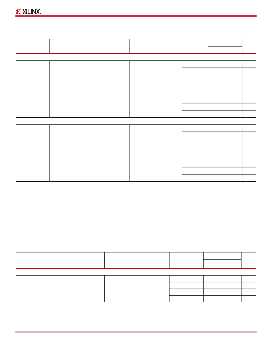
Pin-to-Pin Setup and Hold Times
Input Setup and Hold Times
Table 19: Pin-to-Pin Setup and Hold Times for the IOB Input Path (System Synchronous)
Symbol
Description
Conditions
Device
Speed Grade: -4
Units
Min
Setup Times
TPSDCM
When writing to the Input Flip-Flop (IFF), the
time from the setup of data at the Input pin
to the active transition at a Global Clock pin.
The DCM is in use. No Input Delay is
programmed.
LVCMOS25(2),
IFD_DELAY_VALUE = 0,
with DCM(4)
XA3S200A
2.84
ns
XA3S400A
2.68
ns
XA3S700A
2.57
ns
XA3S1400A
2.17
ns
TPSFD
When writing to IFF, the time from the setup
of data at the Input pin to an active transition
at the Global Clock pin. The DCM is not in
use. The Input Delay is progr ammed.
LVCMOS25(2),
IFD_DELAY_VALUE = 5,
without DCM
XA3S200A
2.76
ns
XA3S400A
2.60
ns
XA3S700A
2.63
ns
XA3S1400A
2.41
ns
Hold Times
TPHDCM
When writing to IFF, the time from the active
transition at the Global Clock pin to the point
when data must be held at the Input pin. The
DCM is in use. No Input Delay is
programmed.
LVCMOS25(3),
IFD_DELAY_VALUE = 0,
with DCM(4)
XA3S200A
–0.52
ns
XA3S400A
–0.29
ns
XA3S700A
–0.12
ns
XA3S1400A
0.00
ns
TPHFD
When writing to IFF, the time from the active
transition at the Global Clock pin to the point
when data must be held at the Input pin. The
DCM is not in use. The Input Delay is
programmed.
LVCMOS25(3),
IFD_DELAY_VALUE = 5,
without DCM
XA3S200A
–0.56
ns
XA3S400A
–0.42
ns
XA3S700A
–0.75
ns
XA3S1400A
–0.69
ns
Notes:
1.
The numbers in this table are tested using the methodology presented in Table 26 and are based on the operating conditions set forth in
2.
This setup time requires adjustment whenever a signal standard other than LVCMOS25 is assigned to the Global Clock Input or the data
Input. If this is true of the Global Clock Input, subtract the appropriate adjustment from Table 22. If this is true of the data Input, add the
appropriate Input adjustment from the same table.
3.
This hold time requires adjustment whenever a signal standard other than LVCMOS25 is assigned to the Global Clock Input or the data
Input. If this is true of the Global Clock Input, add the appropriate Input adjustment from Table 22. If this is true of the data Input, subtract the
appropriate Input adjustment from the same table. When the hold time is negative, it is possible to change the data before the clock’s active
edge.
4.
DCM output jitter is included in all measurements.
Table 20: Setup and Hold Times for the IOB Input Path
Symbol
Description
Conditions
IFD_
DELAY_
VALUE
Device
Speed Grade: -4
Units
Min
Setup Times
TIOPICK
Time from the setup of data at the
Input pin to the active transition at
the ICLK input of the Input
Flip-Flop (IFF). No Input Delay is
programmed.
LVCMOS25(2)
0
XA3S200A
1.81
ns
XA3S400A
1.51
ns
XA3S700A
1.51
ns
XA3S1400A
1.74
ns
相关PDF资料 |
PDF描述 |
|---|---|
| ASM28DTAD | CONN EDGECARD 56POS R/A .156 SLD |
| XA3S1600E-4FG400I | IC FPGA SPARTAN-3E 400FGBGA |
| XA3S1600E-4FGG400I | IC FPGA SPARTAN-3E 1600K 400FBGA |
| ACB91DHRR-S621 | CONN EDGECARD EXTEND 182POS .050 |
| ABB91DHRR-S621 | CONN EDGECARD EXTEND 182POS .050 |
相关代理商/技术参数 |
参数描述 |
|---|---|
| XA3S1400A-4FGG484Q | 功能描述:IC FPGA SPARTAN3A 1400K 484-FBGA RoHS:是 类别:集成电路 (IC) >> 嵌入式 - FPGA(现场可编程门阵列) 系列:Spartan®-3A XA 产品变化通告:Step Intro and Pkg Change 11/March/2008 标准包装:1 系列:Virtex®-5 SXT LAB/CLB数:4080 逻辑元件/单元数:52224 RAM 位总计:4866048 输入/输出数:480 门数:- 电源电压:0.95 V ~ 1.05 V 安装类型:表面贴装 工作温度:-40°C ~ 100°C 封装/外壳:1136-BBGA,FCBGA 供应商设备封装:1136-FCBGA 配用:568-5088-ND - BOARD DEMO DAC1408D750122-1796-ND - EVALUATION PLATFORM VIRTEX-5 |
| XA3S1500-4FGG456I | 功能描述:IC FPGA SPARTAN-3 1.5M 456-FBGA RoHS:是 类别:集成电路 (IC) >> 嵌入式 - FPGA(现场可编程门阵列) 系列:Spartan®-3 XA 产品变化通告:Step Intro and Pkg Change 11/March/2008 标准包装:1 系列:Virtex®-5 SXT LAB/CLB数:4080 逻辑元件/单元数:52224 RAM 位总计:4866048 输入/输出数:480 门数:- 电源电压:0.95 V ~ 1.05 V 安装类型:表面贴装 工作温度:-40°C ~ 100°C 封装/外壳:1136-BBGA,FCBGA 供应商设备封装:1136-FCBGA 配用:568-5088-ND - BOARD DEMO DAC1408D750122-1796-ND - EVALUATION PLATFORM VIRTEX-5 |
| XA3S1500-4FGG676I | 功能描述:IC FPGA SPARTAN-3 1.5M 676-FBGA RoHS:是 类别:集成电路 (IC) >> 嵌入式 - FPGA(现场可编程门阵列) 系列:Spartan®-3 XA 产品变化通告:Step Intro and Pkg Change 11/March/2008 标准包装:1 系列:Virtex®-5 SXT LAB/CLB数:4080 逻辑元件/单元数:52224 RAM 位总计:4866048 输入/输出数:480 门数:- 电源电压:0.95 V ~ 1.05 V 安装类型:表面贴装 工作温度:-40°C ~ 100°C 封装/外壳:1136-BBGA,FCBGA 供应商设备封装:1136-FCBGA 配用:568-5088-ND - BOARD DEMO DAC1408D750122-1796-ND - EVALUATION PLATFORM VIRTEX-5 |
| XA3S1600E-4FG400I | 功能描述:IC FPGA SPARTAN-3E 400FGBGA RoHS:否 类别:集成电路 (IC) >> 嵌入式 - FPGA(现场可编程门阵列) 系列:Spartan®-3E XA 产品变化通告:Step Intro and Pkg Change 11/March/2008 标准包装:1 系列:Virtex®-5 SXT LAB/CLB数:4080 逻辑元件/单元数:52224 RAM 位总计:4866048 输入/输出数:480 门数:- 电源电压:0.95 V ~ 1.05 V 安装类型:表面贴装 工作温度:-40°C ~ 100°C 封装/外壳:1136-BBGA,FCBGA 供应商设备封装:1136-FCBGA 配用:568-5088-ND - BOARD DEMO DAC1408D750122-1796-ND - EVALUATION PLATFORM VIRTEX-5 |
| XA3S1600E-4FGG400I | 功能描述:IC FPGA SPARTAN-3E 1600K 400FBGA RoHS:是 类别:集成电路 (IC) >> 嵌入式 - FPGA(现场可编程门阵列) 系列:Spartan®-3E XA 产品变化通告:Step Intro and Pkg Change 11/March/2008 标准包装:1 系列:Virtex®-5 SXT LAB/CLB数:4080 逻辑元件/单元数:52224 RAM 位总计:4866048 输入/输出数:480 门数:- 电源电压:0.95 V ~ 1.05 V 安装类型:表面贴装 工作温度:-40°C ~ 100°C 封装/外壳:1136-BBGA,FCBGA 供应商设备封装:1136-FCBGA 配用:568-5088-ND - BOARD DEMO DAC1408D750122-1796-ND - EVALUATION PLATFORM VIRTEX-5 |
发布紧急采购,3分钟左右您将得到回复。