参数资料
| 型号: | XA3S1400A-4FGG484I |
| 厂商: | Xilinx Inc |
| 文件页数: | 26/57页 |
| 文件大小: | 0K |
| 描述: | IC FPGA SPARTAN3A 1400K 484-FBGA |
| 标准包装: | 60 |
| 系列: | Spartan®-3A XA |
| LAB/CLB数: | 2816 |
| 逻辑元件/单元数: | 25344 |
| RAM 位总计: | 589824 |
| 输入/输出数: | 375 |
| 门数: | 1400000 |
| 电源电压: | 1.14 V ~ 1.26 V |
| 安装类型: | 表面贴装 |
| 工作温度: | -40°C ~ 100°C |
| 封装/外壳: | 484-BBGA |
| 供应商设备封装: | 484-FBGA |
第1页第2页第3页第4页第5页第6页第7页第8页第9页第10页第11页第12页第13页第14页第15页第16页第17页第18页第19页第20页第21页第22页第23页第24页第25页当前第26页第27页第28页第29页第30页第31页第32页第33页第34页第35页第36页第37页第38页第39页第40页第41页第42页第43页第44页第45页第46页第47页第48页第49页第50页第51页第52页第53页第54页第55页第56页第57页
XA Spartan-3A Automotive FPGA Family Data Sheet
DS681 (v2.0) April 22, 2011
Product Specification
32
Simultaneously Switching Output Guidelines
This section provides guidelines for the recommended maximum allowable number of Simultaneous Switching Outputs
(SSOs). These guidelines describe the maximum number of user I/O pins of a given output signal standard that should
simultaneously switch in the same direction, while maintaining a safe level of switching noise. Meeting these guidelines for
the stated test conditions ensures that the FPGA operates free from the adverse effects of ground and power bounce.
Ground or power bounce occurs when a large number of outputs simultaneously switch in the same direction. The output
drive transistors all conduct current to a common voltage rail. Low-to-High transitions conduct to the VCCO rail; High-to-Low
transitions conduct to the GND rail. The resulting cumulative current transient induces a voltage difference across the
inductance that exists between the die pad and the power supply or ground return. The inductance is associated with
bonding wires, the package lead frame, and any other signal routing inside the package. Other variables contribute to SSO
noise levels, including stray inductance on the PCB as well as capacitive loading at receivers. Any SSO-induced voltage
consequently affects internal switching noise margins and ultimately signal quality.
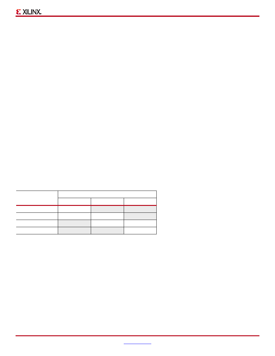
Table 27 and Table 28 provide the essential SSO guidelines. For each device/package combination, Table 27 provides the
number of equivalent VCCO/GND pairs. For each output signal standard and drive strength, Table 28 recommends the
maximum number of SSOs, switching in the same direction, allowed per VCCO/GND pair within an I/O bank. The guidelines
in Table 28 are categorized by package style, slew rate, and output drive current. Furthermore, the number of SSOs is
specified by I/O bank. Generally, the left and right I/O banks (Banks 1 and 3) support higher output drive current.
Multiply the appropriate numbers from Table 27 and Table 28 to calculate the maximum number of SSOs allowed within an
I/O bank. Exceeding these SSO guidelines might result in increased power or ground bounce, degraded signal integrity, or
increased system jitter.
The recommended maximum SSO values assumes that the FPGA is soldered on the printed circuit board and that the board
uses sound design practices. The SSO values do not apply for FPGAs mounted in sockets, due to the lead inductance
introduced by the socket.
Ball grid array packages are recommended for applications with a large number of simultaneously switching outputs.
Table 27: Equivalent VCCO/GND Pairs per Bank
Device
Package Style (Pb-free)
FTG256
FGG400
FGG484
XA3S200A
4
–
XA3S400A
4
5
–
XA3S700A
–55
XA3S1400A
–
–6
相关PDF资料 |
PDF描述 |
|---|---|
| ASM28DTAD | CONN EDGECARD 56POS R/A .156 SLD |
| XA3S1600E-4FG400I | IC FPGA SPARTAN-3E 400FGBGA |
| XA3S1600E-4FGG400I | IC FPGA SPARTAN-3E 1600K 400FBGA |
| ACB91DHRR-S621 | CONN EDGECARD EXTEND 182POS .050 |
| ABB91DHRR-S621 | CONN EDGECARD EXTEND 182POS .050 |
相关代理商/技术参数 |
参数描述 |
|---|---|
| XA3S1400A-4FGG484Q | 功能描述:IC FPGA SPARTAN3A 1400K 484-FBGA RoHS:是 类别:集成电路 (IC) >> 嵌入式 - FPGA(现场可编程门阵列) 系列:Spartan®-3A XA 产品变化通告:Step Intro and Pkg Change 11/March/2008 标准包装:1 系列:Virtex®-5 SXT LAB/CLB数:4080 逻辑元件/单元数:52224 RAM 位总计:4866048 输入/输出数:480 门数:- 电源电压:0.95 V ~ 1.05 V 安装类型:表面贴装 工作温度:-40°C ~ 100°C 封装/外壳:1136-BBGA,FCBGA 供应商设备封装:1136-FCBGA 配用:568-5088-ND - BOARD DEMO DAC1408D750122-1796-ND - EVALUATION PLATFORM VIRTEX-5 |
| XA3S1500-4FGG456I | 功能描述:IC FPGA SPARTAN-3 1.5M 456-FBGA RoHS:是 类别:集成电路 (IC) >> 嵌入式 - FPGA(现场可编程门阵列) 系列:Spartan®-3 XA 产品变化通告:Step Intro and Pkg Change 11/March/2008 标准包装:1 系列:Virtex®-5 SXT LAB/CLB数:4080 逻辑元件/单元数:52224 RAM 位总计:4866048 输入/输出数:480 门数:- 电源电压:0.95 V ~ 1.05 V 安装类型:表面贴装 工作温度:-40°C ~ 100°C 封装/外壳:1136-BBGA,FCBGA 供应商设备封装:1136-FCBGA 配用:568-5088-ND - BOARD DEMO DAC1408D750122-1796-ND - EVALUATION PLATFORM VIRTEX-5 |
| XA3S1500-4FGG676I | 功能描述:IC FPGA SPARTAN-3 1.5M 676-FBGA RoHS:是 类别:集成电路 (IC) >> 嵌入式 - FPGA(现场可编程门阵列) 系列:Spartan®-3 XA 产品变化通告:Step Intro and Pkg Change 11/March/2008 标准包装:1 系列:Virtex®-5 SXT LAB/CLB数:4080 逻辑元件/单元数:52224 RAM 位总计:4866048 输入/输出数:480 门数:- 电源电压:0.95 V ~ 1.05 V 安装类型:表面贴装 工作温度:-40°C ~ 100°C 封装/外壳:1136-BBGA,FCBGA 供应商设备封装:1136-FCBGA 配用:568-5088-ND - BOARD DEMO DAC1408D750122-1796-ND - EVALUATION PLATFORM VIRTEX-5 |
| XA3S1600E-4FG400I | 功能描述:IC FPGA SPARTAN-3E 400FGBGA RoHS:否 类别:集成电路 (IC) >> 嵌入式 - FPGA(现场可编程门阵列) 系列:Spartan®-3E XA 产品变化通告:Step Intro and Pkg Change 11/March/2008 标准包装:1 系列:Virtex®-5 SXT LAB/CLB数:4080 逻辑元件/单元数:52224 RAM 位总计:4866048 输入/输出数:480 门数:- 电源电压:0.95 V ~ 1.05 V 安装类型:表面贴装 工作温度:-40°C ~ 100°C 封装/外壳:1136-BBGA,FCBGA 供应商设备封装:1136-FCBGA 配用:568-5088-ND - BOARD DEMO DAC1408D750122-1796-ND - EVALUATION PLATFORM VIRTEX-5 |
| XA3S1600E-4FGG400I | 功能描述:IC FPGA SPARTAN-3E 1600K 400FBGA RoHS:是 类别:集成电路 (IC) >> 嵌入式 - FPGA(现场可编程门阵列) 系列:Spartan®-3E XA 产品变化通告:Step Intro and Pkg Change 11/March/2008 标准包装:1 系列:Virtex®-5 SXT LAB/CLB数:4080 逻辑元件/单元数:52224 RAM 位总计:4866048 输入/输出数:480 门数:- 电源电压:0.95 V ~ 1.05 V 安装类型:表面贴装 工作温度:-40°C ~ 100°C 封装/外壳:1136-BBGA,FCBGA 供应商设备封装:1136-FCBGA 配用:568-5088-ND - BOARD DEMO DAC1408D750122-1796-ND - EVALUATION PLATFORM VIRTEX-5 |
发布紧急采购,3分钟左右您将得到回复。