参数资料
| 型号: | XA3S1400A-4FGG484I |
| 厂商: | Xilinx Inc |
| 文件页数: | 25/57页 |
| 文件大小: | 0K |
| 描述: | IC FPGA SPARTAN3A 1400K 484-FBGA |
| 标准包装: | 60 |
| 系列: | Spartan®-3A XA |
| LAB/CLB数: | 2816 |
| 逻辑元件/单元数: | 25344 |
| RAM 位总计: | 589824 |
| 输入/输出数: | 375 |
| 门数: | 1400000 |
| 电源电压: | 1.14 V ~ 1.26 V |
| 安装类型: | 表面贴装 |
| 工作温度: | -40°C ~ 100°C |
| 封装/外壳: | 484-BBGA |
| 供应商设备封装: | 484-FBGA |
第1页第2页第3页第4页第5页第6页第7页第8页第9页第10页第11页第12页第13页第14页第15页第16页第17页第18页第19页第20页第21页第22页第23页第24页当前第25页第26页第27页第28页第29页第30页第31页第32页第33页第34页第35页第36页第37页第38页第39页第40页第41页第42页第43页第44页第45页第46页第47页第48页第49页第50页第51页第52页第53页第54页第55页第56页第57页
XA Spartan-3A Automotive FPGA Family Data Sheet
DS681 (v2.0) April 22, 2011
Product Specification
31
The capacitive load (CL) is connected between the output and GND. The Output timing for all standards, as published in the
speed files and the data sheet, is always based on a CL value of zero. High-impedance probes (less than 1 pF) are used for
all measurements. Any delay that the test fixture might contribute to test measurements is subtracted from those
measurements to produce the final timing numbers as published in the speed files and data sheet.
Using IBIS Models to Simulate Load Conditions in Application
IBIS models permit the most accurate prediction of timing delays for a given application. The parameters found in the IBIS
model (VREF, RREF, and VMEAS) correspond directly with the parameters used in Table 26 (VT, RT, and VM). Do not confuse
VREF (the termination voltage) from the IBIS model with VREF (the input-switching threshold) from the table. A fourth
parameter, CREF, is always zero. The four parameters describe all relevant output test conditions. IBIS models are found in
the Xilinx development software as well as at the following link:
Delays for a given application are simulated according to its specific load conditions as follows:
1.
Simulate the desired signal standard with the output driver connected to the test setup shown in Figure 9. Use
2.
Record the time to VM.
3.
Simulate the same signal standard with the output driver connected to the PCB trace with load. Use the appropriate IBIS
model (including VREF, RREF, CREF, and VMEAS values) or capacitive value to represent the load.
4.
Record the time to VMEAS.
5.
Compare the results of steps 2 and 4. Add (or subtract) the increase (or decrease) in delay to (or from) the appropriate
Output standard adjustment (Table 25) to yield the worst-case delay of the PCB trace.
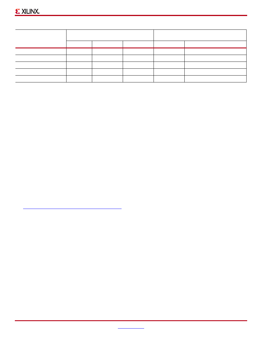
DIFF_SSTL18_II
0.9
VREF – 0.5
VREF + 0.5
50
0.9
VREF
DIFF_SSTL2_I
1.25
VREF – 0.5
VREF + 0.5
50
1.25
VREF
DIFF_SSTL2_II
1.25
VREF – 0.5
VREF + 0.5
50
1.25
VREF
DIFF_SSTL3_I
1.5
VREF – 0.5
VREF + 0.5
50
1.5
VREF
DIFF_SSTL3_II
1.5
VREF – 0.5
VREF + 0.5
50
1.5
VREF
Notes:
1.
Descriptions of the relevant symbols are as follows:
VREF – The reference voltage for setting the input switching threshold
VICM – The common mode input voltage
VM – Voltage of measurement point on signal transition
VL – Low-level test voltage at Input pin
VH – High-level test voltage at Input pin
RT – Effective termination resistance, which takes on a value of 1 M when no parallel termination is required
VT – Termination voltage
2.
The load capacitance (CL) at the Output pin is 0 pF for all signal standards.
3.
According to the PCI specification.
Table 26: Test Methods for Timing Measurement at I/Os (Cont’d)
Signal Standard
(IOSTANDARD)
Inputs
Outputs
Inputs and
Outputs
VREF (V)
VL (V)
VH (V)
RT ()VT (V)
VM (V)
相关PDF资料 |
PDF描述 |
|---|---|
| ASM28DTAD | CONN EDGECARD 56POS R/A .156 SLD |
| XA3S1600E-4FG400I | IC FPGA SPARTAN-3E 400FGBGA |
| XA3S1600E-4FGG400I | IC FPGA SPARTAN-3E 1600K 400FBGA |
| ACB91DHRR-S621 | CONN EDGECARD EXTEND 182POS .050 |
| ABB91DHRR-S621 | CONN EDGECARD EXTEND 182POS .050 |
相关代理商/技术参数 |
参数描述 |
|---|---|
| XA3S1400A-4FGG484Q | 功能描述:IC FPGA SPARTAN3A 1400K 484-FBGA RoHS:是 类别:集成电路 (IC) >> 嵌入式 - FPGA(现场可编程门阵列) 系列:Spartan®-3A XA 产品变化通告:Step Intro and Pkg Change 11/March/2008 标准包装:1 系列:Virtex®-5 SXT LAB/CLB数:4080 逻辑元件/单元数:52224 RAM 位总计:4866048 输入/输出数:480 门数:- 电源电压:0.95 V ~ 1.05 V 安装类型:表面贴装 工作温度:-40°C ~ 100°C 封装/外壳:1136-BBGA,FCBGA 供应商设备封装:1136-FCBGA 配用:568-5088-ND - BOARD DEMO DAC1408D750122-1796-ND - EVALUATION PLATFORM VIRTEX-5 |
| XA3S1500-4FGG456I | 功能描述:IC FPGA SPARTAN-3 1.5M 456-FBGA RoHS:是 类别:集成电路 (IC) >> 嵌入式 - FPGA(现场可编程门阵列) 系列:Spartan®-3 XA 产品变化通告:Step Intro and Pkg Change 11/March/2008 标准包装:1 系列:Virtex®-5 SXT LAB/CLB数:4080 逻辑元件/单元数:52224 RAM 位总计:4866048 输入/输出数:480 门数:- 电源电压:0.95 V ~ 1.05 V 安装类型:表面贴装 工作温度:-40°C ~ 100°C 封装/外壳:1136-BBGA,FCBGA 供应商设备封装:1136-FCBGA 配用:568-5088-ND - BOARD DEMO DAC1408D750122-1796-ND - EVALUATION PLATFORM VIRTEX-5 |
| XA3S1500-4FGG676I | 功能描述:IC FPGA SPARTAN-3 1.5M 676-FBGA RoHS:是 类别:集成电路 (IC) >> 嵌入式 - FPGA(现场可编程门阵列) 系列:Spartan®-3 XA 产品变化通告:Step Intro and Pkg Change 11/March/2008 标准包装:1 系列:Virtex®-5 SXT LAB/CLB数:4080 逻辑元件/单元数:52224 RAM 位总计:4866048 输入/输出数:480 门数:- 电源电压:0.95 V ~ 1.05 V 安装类型:表面贴装 工作温度:-40°C ~ 100°C 封装/外壳:1136-BBGA,FCBGA 供应商设备封装:1136-FCBGA 配用:568-5088-ND - BOARD DEMO DAC1408D750122-1796-ND - EVALUATION PLATFORM VIRTEX-5 |
| XA3S1600E-4FG400I | 功能描述:IC FPGA SPARTAN-3E 400FGBGA RoHS:否 类别:集成电路 (IC) >> 嵌入式 - FPGA(现场可编程门阵列) 系列:Spartan®-3E XA 产品变化通告:Step Intro and Pkg Change 11/March/2008 标准包装:1 系列:Virtex®-5 SXT LAB/CLB数:4080 逻辑元件/单元数:52224 RAM 位总计:4866048 输入/输出数:480 门数:- 电源电压:0.95 V ~ 1.05 V 安装类型:表面贴装 工作温度:-40°C ~ 100°C 封装/外壳:1136-BBGA,FCBGA 供应商设备封装:1136-FCBGA 配用:568-5088-ND - BOARD DEMO DAC1408D750122-1796-ND - EVALUATION PLATFORM VIRTEX-5 |
| XA3S1600E-4FGG400I | 功能描述:IC FPGA SPARTAN-3E 1600K 400FBGA RoHS:是 类别:集成电路 (IC) >> 嵌入式 - FPGA(现场可编程门阵列) 系列:Spartan®-3E XA 产品变化通告:Step Intro and Pkg Change 11/March/2008 标准包装:1 系列:Virtex®-5 SXT LAB/CLB数:4080 逻辑元件/单元数:52224 RAM 位总计:4866048 输入/输出数:480 门数:- 电源电压:0.95 V ~ 1.05 V 安装类型:表面贴装 工作温度:-40°C ~ 100°C 封装/外壳:1136-BBGA,FCBGA 供应商设备封装:1136-FCBGA 配用:568-5088-ND - BOARD DEMO DAC1408D750122-1796-ND - EVALUATION PLATFORM VIRTEX-5 |
发布紧急采购,3分钟左右您将得到回复。