参数资料
| 型号: | XA3S1400A-4FGG484I |
| 厂商: | Xilinx Inc |
| 文件页数: | 12/57页 |
| 文件大小: | 0K |
| 描述: | IC FPGA SPARTAN3A 1400K 484-FBGA |
| 标准包装: | 60 |
| 系列: | Spartan®-3A XA |
| LAB/CLB数: | 2816 |
| 逻辑元件/单元数: | 25344 |
| RAM 位总计: | 589824 |
| 输入/输出数: | 375 |
| 门数: | 1400000 |
| 电源电压: | 1.14 V ~ 1.26 V |
| 安装类型: | 表面贴装 |
| 工作温度: | -40°C ~ 100°C |
| 封装/外壳: | 484-BBGA |
| 供应商设备封装: | 484-FBGA |
第1页第2页第3页第4页第5页第6页第7页第8页第9页第10页第11页当前第12页第13页第14页第15页第16页第17页第18页第19页第20页第21页第22页第23页第24页第25页第26页第27页第28页第29页第30页第31页第32页第33页第34页第35页第36页第37页第38页第39页第40页第41页第42页第43页第44页第45页第46页第47页第48页第49页第50页第51页第52页第53页第54页第55页第56页第57页
XA Spartan-3A Automotive FPGA Family Data Sheet
DS681 (v2.0) April 22, 2011
Product Specification
2
Key Feature Differences from Commercial XC Devices
AEC-Q100 device qualification and full production part approval process (PPAP) documentation support available in
both extended temperature I- and Q-Grades
Guaranteed to meet full electrical specification over the TJ = –40°C to +125°C temperature range (Q-Grade)
XA Spartan-3A devices are available in the -4 speed grade only
PCI-66 is not supported in the XA Spartan-3A FPGA product line
Platform Flash is not supported within the XA family
XA Spartan-3A devices are available in Pb-Free packaging only.
MultiBoot is not supported in XA versions of this product.
The XA Spartan-3A device must be power cycled prior to reconfiguration.
Architectural Overview
The XA Spartan-3A family architecture consists of five fundamental programmable functional elements:
Configurable Logic Blocks (CLBs) contain flexible Look-Up Tables (LUTs) that implement logic plus storage
elements used as flip-flops or latches. CLBs perform a wide variety of logical functions as well as store data.
Input/Output Blocks (IOBs) control the flow of data between the I/O pins and the internal logic of the device. IOBs
support bidirectional data flow plus 3-state operation. Supports a variety of signal standards, including several
high-performance differential standards. Double Data-Rate (DDR) registers are included.
Block RAM provides data storage in the form of 18-Kb dual-port blocks.
Multiplier Blocks accept two 18-bit binary numbers as inputs and calculate the product.
Digital Clock Manager (DCM) Blocks provide self-calibrating, fully digital solutions for distributing, delaying,
multiplying, dividing, and phase-shifting clock signals.These elements are organized as shown in Figure 1. A dual ring
of staggered IOBs surrounds a regular array of CLBs. Each device has two columns of block RAM. Each RAM column
consists of several 18-Kb RAM blocks. Each block RAM is associated with a dedicated multiplier. The DCMs are
positioned in the center with two at the top and two at the bottom of the device. The XA3S700A and XA3S1400A add
two DCMs in the middle of the two columns of block RAM and multipliers. The XA Spartan-3A family features a rich
network of routing that interconnect all five functional elements, transmitting signals among them. Each functional
element has an associated switch matrix that permits multiple connections to the routing.
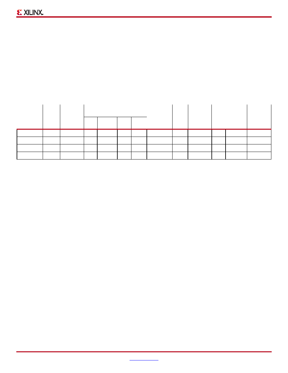
Table 1: Summary of XA Spartan-3A FPGA Attributes)
Device
System
Gates
Equivalent
Logic
Cells
CLB Array
(One CLB = Four Slices)
Distributed
RAM bits(1)
Block
RAM
bits(1)
Dedicated
Multipliers
DCMs
Maximum
User I/O
Maximum
Differential
I/O Pairs
Rows Columns
Total
CLBs
Total
Slices
XA3S200A
200K
4,032
32
16
448
1,792
28K
288K
16
4
195
90
XA3S400A
400K
8,064
40
24
896
3,584
56K
360K
20
4
311
142
XA3S700A
700K
13,248
48
32
1,472
5,888
92K
360K
20
8
372
165
XA3S1400A 1400K
25,344
72
40
2,816 11,264
176K
576K
32
8
375
165
Notes:
1.
By convention, one Kb is equivalent to 1,024 bits.
相关PDF资料 |
PDF描述 |
|---|---|
| ASM28DTAD | CONN EDGECARD 56POS R/A .156 SLD |
| XA3S1600E-4FG400I | IC FPGA SPARTAN-3E 400FGBGA |
| XA3S1600E-4FGG400I | IC FPGA SPARTAN-3E 1600K 400FBGA |
| ACB91DHRR-S621 | CONN EDGECARD EXTEND 182POS .050 |
| ABB91DHRR-S621 | CONN EDGECARD EXTEND 182POS .050 |
相关代理商/技术参数 |
参数描述 |
|---|---|
| XA3S1400A-4FGG484Q | 功能描述:IC FPGA SPARTAN3A 1400K 484-FBGA RoHS:是 类别:集成电路 (IC) >> 嵌入式 - FPGA(现场可编程门阵列) 系列:Spartan®-3A XA 产品变化通告:Step Intro and Pkg Change 11/March/2008 标准包装:1 系列:Virtex®-5 SXT LAB/CLB数:4080 逻辑元件/单元数:52224 RAM 位总计:4866048 输入/输出数:480 门数:- 电源电压:0.95 V ~ 1.05 V 安装类型:表面贴装 工作温度:-40°C ~ 100°C 封装/外壳:1136-BBGA,FCBGA 供应商设备封装:1136-FCBGA 配用:568-5088-ND - BOARD DEMO DAC1408D750122-1796-ND - EVALUATION PLATFORM VIRTEX-5 |
| XA3S1500-4FGG456I | 功能描述:IC FPGA SPARTAN-3 1.5M 456-FBGA RoHS:是 类别:集成电路 (IC) >> 嵌入式 - FPGA(现场可编程门阵列) 系列:Spartan®-3 XA 产品变化通告:Step Intro and Pkg Change 11/March/2008 标准包装:1 系列:Virtex®-5 SXT LAB/CLB数:4080 逻辑元件/单元数:52224 RAM 位总计:4866048 输入/输出数:480 门数:- 电源电压:0.95 V ~ 1.05 V 安装类型:表面贴装 工作温度:-40°C ~ 100°C 封装/外壳:1136-BBGA,FCBGA 供应商设备封装:1136-FCBGA 配用:568-5088-ND - BOARD DEMO DAC1408D750122-1796-ND - EVALUATION PLATFORM VIRTEX-5 |
| XA3S1500-4FGG676I | 功能描述:IC FPGA SPARTAN-3 1.5M 676-FBGA RoHS:是 类别:集成电路 (IC) >> 嵌入式 - FPGA(现场可编程门阵列) 系列:Spartan®-3 XA 产品变化通告:Step Intro and Pkg Change 11/March/2008 标准包装:1 系列:Virtex®-5 SXT LAB/CLB数:4080 逻辑元件/单元数:52224 RAM 位总计:4866048 输入/输出数:480 门数:- 电源电压:0.95 V ~ 1.05 V 安装类型:表面贴装 工作温度:-40°C ~ 100°C 封装/外壳:1136-BBGA,FCBGA 供应商设备封装:1136-FCBGA 配用:568-5088-ND - BOARD DEMO DAC1408D750122-1796-ND - EVALUATION PLATFORM VIRTEX-5 |
| XA3S1600E-4FG400I | 功能描述:IC FPGA SPARTAN-3E 400FGBGA RoHS:否 类别:集成电路 (IC) >> 嵌入式 - FPGA(现场可编程门阵列) 系列:Spartan®-3E XA 产品变化通告:Step Intro and Pkg Change 11/March/2008 标准包装:1 系列:Virtex®-5 SXT LAB/CLB数:4080 逻辑元件/单元数:52224 RAM 位总计:4866048 输入/输出数:480 门数:- 电源电压:0.95 V ~ 1.05 V 安装类型:表面贴装 工作温度:-40°C ~ 100°C 封装/外壳:1136-BBGA,FCBGA 供应商设备封装:1136-FCBGA 配用:568-5088-ND - BOARD DEMO DAC1408D750122-1796-ND - EVALUATION PLATFORM VIRTEX-5 |
| XA3S1600E-4FGG400I | 功能描述:IC FPGA SPARTAN-3E 1600K 400FBGA RoHS:是 类别:集成电路 (IC) >> 嵌入式 - FPGA(现场可编程门阵列) 系列:Spartan®-3E XA 产品变化通告:Step Intro and Pkg Change 11/March/2008 标准包装:1 系列:Virtex®-5 SXT LAB/CLB数:4080 逻辑元件/单元数:52224 RAM 位总计:4866048 输入/输出数:480 门数:- 电源电压:0.95 V ~ 1.05 V 安装类型:表面贴装 工作温度:-40°C ~ 100°C 封装/外壳:1136-BBGA,FCBGA 供应商设备封装:1136-FCBGA 配用:568-5088-ND - BOARD DEMO DAC1408D750122-1796-ND - EVALUATION PLATFORM VIRTEX-5 |
发布紧急采购,3分钟左右您将得到回复。