参数资料
| 型号: | XC2S100-5FGG256C |
| 厂商: | Xilinx Inc |
| 文件页数: | 36/99页 |
| 文件大小: | 0K |
| 描述: | IC SPARTAN-II FPGA 100K 256-FBGA |
| 标准包装: | 90 |
| 系列: | Spartan®-II |
| LAB/CLB数: | 600 |
| 逻辑元件/单元数: | 2700 |
| RAM 位总计: | 40960 |
| 输入/输出数: | 176 |
| 门数: | 100000 |
| 电源电压: | 2.375 V ~ 2.625 V |
| 安装类型: | 表面贴装 |
| 工作温度: | 0°C ~ 85°C |
| 封装/外壳: | 256-BGA |
| 供应商设备封装: | 256-FBGA(17x17) |
| 其它名称: | 122-1302 |
第1页第2页第3页第4页第5页第6页第7页第8页第9页第10页第11页第12页第13页第14页第15页第16页第17页第18页第19页第20页第21页第22页第23页第24页第25页第26页第27页第28页第29页第30页第31页第32页第33页第34页第35页当前第36页第37页第38页第39页第40页第41页第42页第43页第44页第45页第46页第47页第48页第49页第50页第51页第52页第53页第54页第55页第56页第57页第58页第59页第60页第61页第62页第63页第64页第65页第66页第67页第68页第69页第70页第71页第72页第73页第74页第75页第76页第77页第78页第79页第80页第81页第82页第83页第84页第85页第86页第87页第88页第89页第90页第91页第92页第93页第94页第95页第96页第97页第98页第99页
Spartan-II FPGA Family: Functional Description
DS001-2 (v2.8) June 13, 2008
Module 2 of 4
Product Specification
41
R
IOBUF_<slew_rate>_<drive_strength>
<slew_rate> can be either F (Fast), or S (Slow) and
<drive_strength> is specified in milliamps (2, 4, 6, 8, 12, 16,
or 24).
When the IOBUF primitive supports an I/O standard such
as LVTTL, LVCMOS, or PCI33_5, the IBUF automatically
configures as a 5V tolerant input buffer unless the VCCO for
the bank is less than 2V. If the single-ended IBUF is placed
in a bank with an HSTL standard (VCCO < 2V), the input
buffer is not 5V tolerant.
The voltage reference signal is "banked" within the
Spartan-II device on a half-edge basis such that for all
packages there are eight independent VREF banks
internally. See Figure 36, page 39 for a representation of
the Spartan-II FPGA I/O banks. Within each bank
approximately one of every six I/O pins is automatically
configured as a VREF input.
Additional restrictions on the Versatile I/O IOBUF
placement require that within a given VCCO bank each
IOBUF must share the same output source drive voltage.
Input buffers of any type and output buffers that do not
require VCCO can be placed within the same VCCO bank.
The LOC property can specify a location for the IOBUF.
An optional delay element is associated with the input path
in each IOBUF. When the IOBUF drives an input flip-flop
within the IOB, the delay element activates by default to
ensure a zero hold-time requirement. Override this default
with the NODELAY=TRUE property.
In the case when the IOBUF does not drive an input flip-flop
within the IOB, the delay element de-activates by default to
provide higher performance. To delay the input signal,
activate the delay element with the DELAY=TRUE property.
3-state output buffers and bidirectional buffers can have
either a weak pull-up resistor, a weak pull-down resistor, or
a weak "keeper" circuit. Control this feature by adding the
appropriate primitive to the output net of the IOBUF
(PULLUP, PULLDOWN, or KEEPER).
Versatile I/O Properties
Access to some of the Versatile I/O features (for example,
location constraints, input delay, output drive strength, and
slew rate) is available through properties associated with
these features.
Input Delay Properties
An optional delay element is associated with each IBUF.
When the IBUF drives a flip-flop within the IOB, the delay
element activates by default to ensure a zero hold-time
requirement. Use the NODELAY=TRUE property to
override this default.
In the case when the IBUF does not drive a flip-flop within
the IOB, the delay element by default de-activates to
provide higher performance. To delay the input signal,
activate the delay element with the DELAY=TRUE property.
IOB Flip-Flop/Latch Property
The I/O Block (IOB) includes an optional register on the
input path, an optional register on the output path, and an
optional register on the 3-state control pin. The design
implementation software automatically takes advantage of
these registers when the following option for the Map
program is specified:
map -pr b <filename>
Alternatively, the IOB = TRUE property can be placed on a
register to force the mapper to place the register in an IOB.
Location Constraints
Specify the location of each Versatile I/O primitive with the
location constraint LOC attached to the Versatile I/O
primitive. The external port identifier indicates the value of
the location constrain. The format of the port identifier
depends on the package chosen for the specific design.
The LOC properties use the following form:
LOC=A42
LOC=P37
Output Slew Rate Property
In the case of the LVTTL output buffers (OBUF, OBUFT, and
IOBUF), slew rate control can be programmed with the
SLEW= property. By default, the slew rate for each output
buffer is reduced to minimize power bus transients when
switching non-critical signals. The SLEW= property has one
of the two following values.
SLEW=SLOW
SLEW=FAST
Output Drive Strength Property
For the LVTTL output buffers (OBUF, OBUFT, and IOBUF,
the desired drive strength can be specified with the DRIVE=
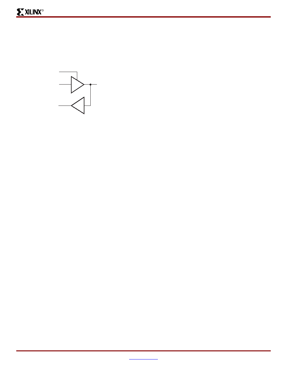
Figure 40: Input/Output Buffer Primitiveprimitive
(IOBUF)
IO
I
IOBUF
DS001_40_061200
T
O
相关PDF资料 |
PDF描述 |
|---|---|
| AMM24DTBT | CONN EDGECARD 48POS R/A .156 SLD |
| AMM24DTAT | CONN EDGECARD 48POS R/A .156 SLD |
| AMC31DRXS-S734 | CONN EDGECARD 62POS DIP .100 SLD |
| ABC60DRXN-S734 | CONN EDGECARD 120PS DIP .100 SLD |
| ABC60DRXH-S734 | CONN EDGECARD 120PS DIP .100 SLD |
相关代理商/技术参数 |
参数描述 |
|---|---|
| XC2S100-5FGG256I | 功能描述:IC SPARTAN-II FPGA 100K 256-FBGA RoHS:是 类别:集成电路 (IC) >> 嵌入式 - FPGA(现场可编程门阵列) 系列:Spartan®-II 标准包装:40 系列:Spartan® 6 LX LAB/CLB数:3411 逻辑元件/单元数:43661 RAM 位总计:2138112 输入/输出数:358 门数:- 电源电压:1.14 V ~ 1.26 V 安装类型:表面贴装 工作温度:-40°C ~ 100°C 封装/外壳:676-BGA 供应商设备封装:676-FBGA(27x27) |
| XC2S100-5FGG456C | 制造商:XILINX 制造商全称:XILINX 功能描述:Spartan-II FPGA Family |
| XC2S100-5FGG456I | 制造商:XILINX 制造商全称:XILINX 功能描述:Spartan-II FPGA Family |
| XC2S100-5PQ208C | 功能描述:IC FPGA 2.5V 600 CLB'S 208-PQFP RoHS:否 类别:集成电路 (IC) >> 嵌入式 - FPGA(现场可编程门阵列) 系列:Spartan®-II 标准包装:40 系列:Spartan® 6 LX LAB/CLB数:3411 逻辑元件/单元数:43661 RAM 位总计:2138112 输入/输出数:358 门数:- 电源电压:1.14 V ~ 1.26 V 安装类型:表面贴装 工作温度:-40°C ~ 100°C 封装/外壳:676-BGA 供应商设备封装:676-FBGA(27x27) |
| XC2S1005PQ208I | 制造商:Xilinx 功能描述: |
发布紧急采购,3分钟左右您将得到回复。