- 您现在的位置:买卖IC网 > PDF目录205934 > XC5204-6PQ240C (Xilinx, Inc.) Field Programmable Gate Arrays PDF资料下载
参数资料
| 型号: | XC5204-6PQ240C |
| 厂商: | Xilinx, Inc. |
| 英文描述: | Field Programmable Gate Arrays |
| 中文描述: | 现场可编程门阵列 |
| 文件页数: | 15/73页 |
| 文件大小: | 598K |
| 代理商: | XC5204-6PQ240C |
第1页第2页第3页第4页第5页第6页第7页第8页第9页第10页第11页第12页第13页第14页当前第15页第16页第17页第18页第19页第20页第21页第22页第23页第24页第25页第26页第27页第28页第29页第30页第31页第32页第33页第34页第35页第36页第37页第38页第39页第40页第41页第42页第43页第44页第45页第46页第47页第48页第49页第50页第51页第52页第53页第54页第55页第56页第57页第58页第59页第60页第61页第62页第63页第64页第65页第66页第67页第68页第69页第70页第71页第72页第73页
R
XC5200 Series Field Programmable Gate Arrays
7-104
November 5, 1998 (Version 5.2)
Configuration
Configuration is the process of loading design-specific pro-
gramming data into one or more FPGAs to define the func-
tional
operation
of
the
internal
blocks
and
their
interconnections. This is somewhat like loading the com-
mand registers of a programmable peripheral chip.
XC5200-Series devices use several hundred bits of config-
uration data per CLB and its associated interconnects.
Each configuration bit defines the state of a static memory
cell that controls either a function look-up table bit, a multi-
plexer input, or an interconnect pass transistor. The devel-
opment system translates the design into a netlist file. It
automatically partitions, places and routes the logic and
generates the configuration data in PROM format.
Special Purpose Pins
Three configuration mode pins (M2, M1, M0) are sampled
prior to configuration to determine the configuration mode.
After configuration, these pins can be used as auxiliary I/O
connections. The development system does not use these
resources unless they are explicitly specified in the design
entry. This is done by placing a special pad symbol called
MD2, MD1, or MD0 instead of the input or output pad sym-
bol.
In XC5200-Series devices, the mode pins have weak
pull-up resistors during configuration. With all three mode
pins High, Slave Serial mode is selected, which is the most
popular configuration mode. Therefore, for the most com-
mon configuration mode, the mode pins can be left uncon-
nected. (Note, however, that the internal pull-up resistor
value can be as high as 100 k
.) After configuration, these
pins can individually have weak pull-up or pull-down resis-
tors, as specified in the design. A pull-down resistor value
of 3.3k
is recommended.
These pins are located in the lower left chip corner and are
near the readback nets. This location allows convenient
routing if compatibility with the XC2000 and XC3000 family
conventions of M0/RT, M1/RD is desired.
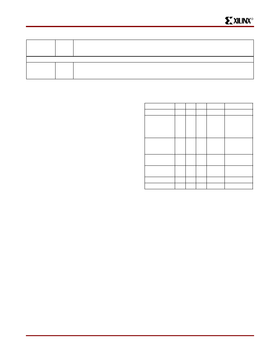
Configuration Modes
XC5200 devices have seven configuration modes. These
modes are selected by a 3-bit input code applied to the M2,
M1, and M0 inputs. There are three self-loading Master
modes, two Peripheral modes, and a Serial Slave mode,
Note :*Peripheral Synchronous can be considered byte-wide
Slave Parallel
which is used primarily for daisy-chained devices. The sev-
enth mode, called Express mode, is an additional slave
mode that allows high-speed parallel configuration. The
coding for mode selection is shown in Table 10.
Note that the smallest package, VQ64, only supports the
Master Serial, Slave Serial, and Express modes.A detailed
description of each configuration mode, with timing infor-
mation, is included later in this data sheet. During configu-
ration, some of the I/O pins are used temporarily for the
configuration process.
All pins used during configuration
are shown in Table 13 on page 124.
Master Modes
The three Master modes use an internal oscillator to gener-
ate a Configuration Clock (CCLK) for driving potential slave
devices. They also generate address and timing for exter-
nal PROM(s) containing the configuration data.
Master Parallel (Up or Down) modes generate the CCLK
signal and PROM addresses and receive byte parallel
data.
The data is internally serialized into the FPGA
data-frame format. The up and down selection generates
starting addresses at either zero or 3FFFF, for compatibility
with different microprocessor addressing conventions. The
Unrestricted User-Programmable I/O Pins
I/O
Weak
Pull-up
I/O
These pins can be configured to be input and/or output after configuration is completed.
Before configuration is completed, these pins have an internal high-value pull-up resis-
tor (20 k
- 100 k) that defines the logic level as High.
Table 9: Pin Descriptions (Continued)
Pin Name
I/O
During
Config.
I/O
After
Config.
Pin Description
Table 10: Configuration Modes
Mode
M2
M1
M0
CCLK
Data
Master Serial
0
output
Bit-Serial
Slave Serial
1
input
Bit-Serial
Master
Parallel Up
1
0
output
Byte-Wide,
increment
from 00000
Master
Parallel Down
1
0
output
Byte-Wide,
decrement
from 3FFFF
Peripheral
Synchronous*
0
1
input
Byte-Wide
Peripheral
Asynchronous
1
0
1
output
Byte-Wide
Express
0
1
0
input
Byte-Wide
Reserved
001
——
相关PDF资料 |
PDF描述 |
|---|---|
| XC5204-6TQ176C | Field Programmable Gate Arrays |
| XC5204-6VQ64C | Field Programmable Gate Arrays |
| XC5204-3TQ144C | Field Programmable Gate Arrays |
| XC5204-3VQ100C | Field Programmable Gate Arrays |
| XC5204-4PC84C | Field Programmable Gate Arrays |
相关代理商/技术参数 |
参数描述 |
|---|---|
| XC5204-6PQG160C | 制造商:Xilinx 功能描述:XC5204-6PQG160C, FPGA XC5200 FAMILY 6K GATES 480 CELLS - Trays 制造商:Xilinx 功能描述:Xilinx XC5204-6PQG160C, FPGA XC5200 Family 6K Gates 480 Cells 83MHz 0.5um (CMOS) Technology 5V 160-Pin PQFP |
| XC5204-6TQ144C | 功能描述:IC FPGA 120 CLB'S 144-TQFP RoHS:否 类别:集成电路 (IC) >> 嵌入式 - FPGA(现场可编程门阵列) 系列:XC5200 产品变化通告:XC4000(E,L) Discontinuation 01/April/2002 标准包装:24 系列:XC4000E/X LAB/CLB数:100 逻辑元件/单元数:238 RAM 位总计:3200 输入/输出数:80 门数:3000 电源电压:4.5 V ~ 5.5 V 安装类型:表面贴装 工作温度:-40°C ~ 100°C 封装/外壳:120-BCBGA 供应商设备封装:120-CPGA(34.55x34.55) |
| XC5204-6TQ144I | 制造商:Xilinx 功能描述: |
| XC5204-6TQ176C | 制造商:XILINX 制造商全称:XILINX 功能描述:Field Programmable Gate Arrays |
| XC5204-6VQ100C | 功能描述:IC FPGA 120 CLB'S 100-VQFP RoHS:否 类别:集成电路 (IC) >> 嵌入式 - FPGA(现场可编程门阵列) 系列:XC5200 产品变化通告:XC4000(E,L) Discontinuation 01/April/2002 标准包装:24 系列:XC4000E/X LAB/CLB数:100 逻辑元件/单元数:238 RAM 位总计:3200 输入/输出数:80 门数:3000 电源电压:4.5 V ~ 5.5 V 安装类型:表面贴装 工作温度:-40°C ~ 100°C 封装/外壳:120-BCBGA 供应商设备封装:120-CPGA(34.55x34.55) |
发布紧急采购,3分钟左右您将得到回复。