- 您现在的位置:买卖IC网 > PDF目录205934 > XC5204-6PQ240C (Xilinx, Inc.) Field Programmable Gate Arrays PDF资料下载
参数资料
| 型号: | XC5204-6PQ240C |
| 厂商: | Xilinx, Inc. |
| 英文描述: | Field Programmable Gate Arrays |
| 中文描述: | 现场可编程门阵列 |
| 文件页数: | 72/73页 |
| 文件大小: | 598K |
| 代理商: | XC5204-6PQ240C |
第1页第2页第3页第4页第5页第6页第7页第8页第9页第10页第11页第12页第13页第14页第15页第16页第17页第18页第19页第20页第21页第22页第23页第24页第25页第26页第27页第28页第29页第30页第31页第32页第33页第34页第35页第36页第37页第38页第39页第40页第41页第42页第43页第44页第45页第46页第47页第48页第49页第50页第51页第52页第53页第54页第55页第56页第57页第58页第59页第60页第61页第62页第63页第64页第65页第66页第67页第68页第69页第70页第71页当前第72页第73页
R
XC5200 Series Field Programmable Gate Arrays
7-90
November 5, 1998 (Version 5.2)
can also be independently disabled for any flip-flop. CLR is
active High. It is not invertible within the CLB.
Global Reset
A separate Global Reset line clears each storage element
during power-up, reconfiguration, or when a dedicated
Reset net is driven active. This global net (GR) does not
compete with other routing resources; it uses a dedicated
distribution network.
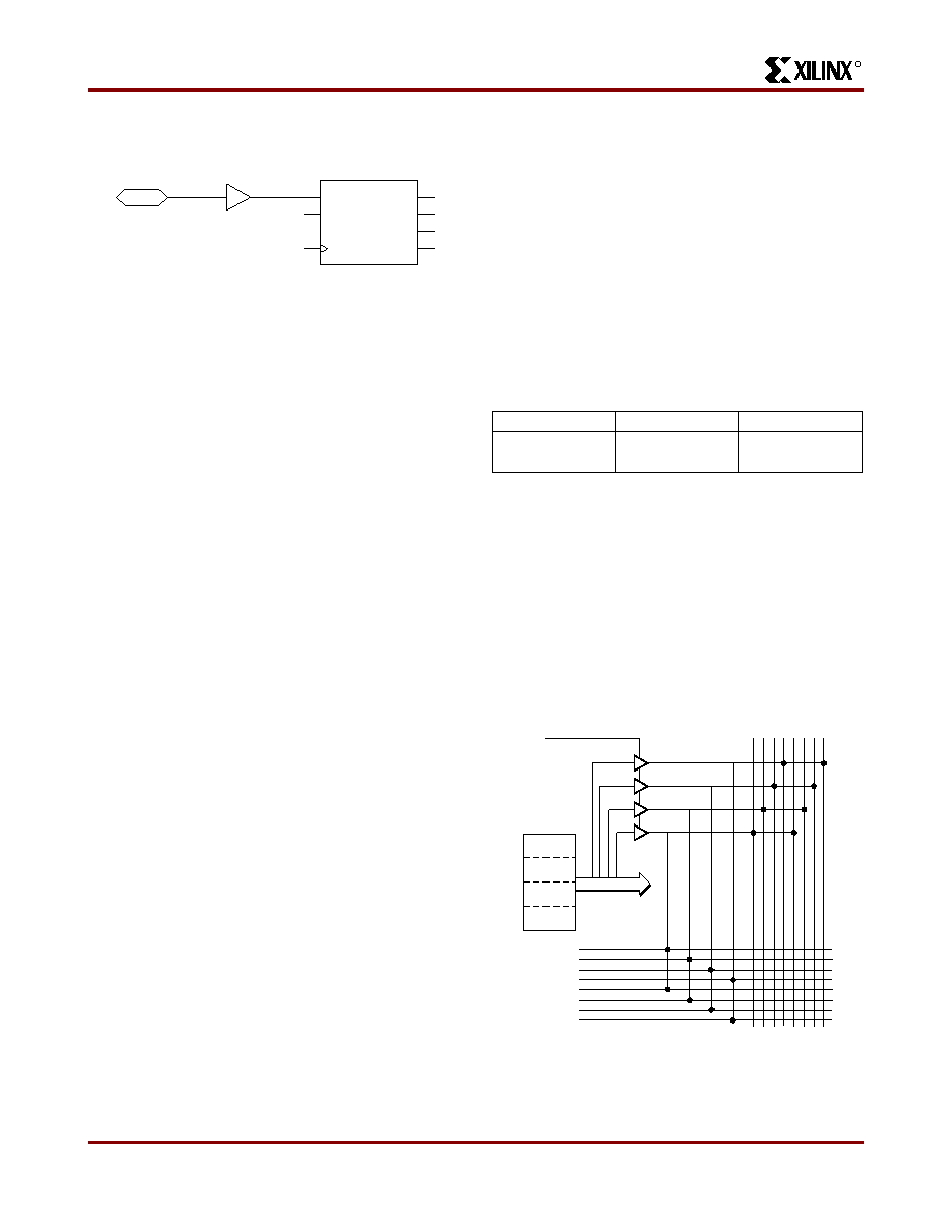
GR can be driven from any user-programmable pin as a
global reset input. To use this global net, place an input pad
and input buffer in the schematic or HDL code, driving the
GR pin of the STARTUP symbol. (See Figure 9.) A specific
pin location can be assigned to this input using a LOC
attribute or property, just as with any other user-program-
mable pad. An inverter can optionally be inserted after the
input buffer to invert the sense of the Global Reset signal.
Alternatively, GR can be driven from any internal node.
Using FPGA Flip-Flops and Latches
The abundance of flip-flops in the XC5200 Series invites
pipelined designs. This is a powerful way of increasing per-
formance by breaking the function into smaller subfunc-
tions and executing them in parallel, passing on the results
through pipeline flip-flops. This method should be seriously
considered wherever throughput is more important than
latency.
To include a CLB flip-flop, place the appropriate library
symbol. For example, FDCE is a D-type flip-flop with clock
enable and asynchronous clear. The corresponding latch
symbol is called LDCE.
In XC5200-Series devices, the flip-flops can be used as
registers or shift registers without blocking the function
generators from performing a different, perhaps unrelated
task. This ability increases the functional capacity of the
devices.
The CLB setup time is specified between the function gen-
erator inputs and the clock input CK. Therefore, the speci-
fied CLB flip-flop setup time includes the delay through the
function generator.
Three-State Buffers
The XC5200 family has four dedicated Three-State Buffers
(TBUFs, or BUFTs in the schematic library) per CLB (see
Figure 9). The four buffers are individually configurable
through four configuration bits to operate as simple
non-inverting buffers or in 3-state mode. When in 3-state
mode the CLB output enable (TS) control signal drives the
enable to all four buffers. Each TBUF can drive up to two
horizontal and/or two vertical Longlines. These 3-state buff-
ers can be used to implement multiplexed or bidirectional
buses on the horizontal or vertical longlines, saving logic
resources.
The 3-state buffer enable is an active-High 3-state (i.e. an
active-Low enable), as shown in Table 4.
Another 3-state buffer with similar access is located near
each I/O block along the right and left edges of the array.
The longlines driven by the 3-state buffers have a weak
keeper at each end. This circuit prevents undefined float-
ing levels.
However, it is overridden by any driver. To
ensure the longline goes high when no buffers are on, add
an additional BUFT to drive the output High during all of the
previously undefined states.
Figure 10 shows how to use the 3-state buffers to imple-
ment a multiplexer. The selection is accomplished by the
buffer 3-state signal.
PAD
IBUF
GR
GTS
CLK DONEIN
Q1Q4
Q2
Q3
STARTUP
X9009
Figure 8: Schematic Symbols for Global Reset
Table 4: Three-State Buffer Functionality
IN
T
OUT
X1
Z
IN
0
IN
CLB
TS
LC3
LC2
LC1
LC0
CLB
Horizontal
Longlines
X9030
Figure 9: XC5200 3-State Buffers
相关PDF资料 |
PDF描述 |
|---|---|
| XC5204-6TQ176C | Field Programmable Gate Arrays |
| XC5204-6VQ64C | Field Programmable Gate Arrays |
| XC5204-3TQ144C | Field Programmable Gate Arrays |
| XC5204-3VQ100C | Field Programmable Gate Arrays |
| XC5204-4PC84C | Field Programmable Gate Arrays |
相关代理商/技术参数 |
参数描述 |
|---|---|
| XC5204-6PQG160C | 制造商:Xilinx 功能描述:XC5204-6PQG160C, FPGA XC5200 FAMILY 6K GATES 480 CELLS - Trays 制造商:Xilinx 功能描述:Xilinx XC5204-6PQG160C, FPGA XC5200 Family 6K Gates 480 Cells 83MHz 0.5um (CMOS) Technology 5V 160-Pin PQFP |
| XC5204-6TQ144C | 功能描述:IC FPGA 120 CLB'S 144-TQFP RoHS:否 类别:集成电路 (IC) >> 嵌入式 - FPGA(现场可编程门阵列) 系列:XC5200 产品变化通告:XC4000(E,L) Discontinuation 01/April/2002 标准包装:24 系列:XC4000E/X LAB/CLB数:100 逻辑元件/单元数:238 RAM 位总计:3200 输入/输出数:80 门数:3000 电源电压:4.5 V ~ 5.5 V 安装类型:表面贴装 工作温度:-40°C ~ 100°C 封装/外壳:120-BCBGA 供应商设备封装:120-CPGA(34.55x34.55) |
| XC5204-6TQ144I | 制造商:Xilinx 功能描述: |
| XC5204-6TQ176C | 制造商:XILINX 制造商全称:XILINX 功能描述:Field Programmable Gate Arrays |
| XC5204-6VQ100C | 功能描述:IC FPGA 120 CLB'S 100-VQFP RoHS:否 类别:集成电路 (IC) >> 嵌入式 - FPGA(现场可编程门阵列) 系列:XC5200 产品变化通告:XC4000(E,L) Discontinuation 01/April/2002 标准包装:24 系列:XC4000E/X LAB/CLB数:100 逻辑元件/单元数:238 RAM 位总计:3200 输入/输出数:80 门数:3000 电源电压:4.5 V ~ 5.5 V 安装类型:表面贴装 工作温度:-40°C ~ 100°C 封装/外壳:120-BCBGA 供应商设备封装:120-CPGA(34.55x34.55) |
发布紧急采购,3分钟左右您将得到回复。