- 您现在的位置:买卖IC网 > PDF目录205934 > XC5204-6PQ240C (Xilinx, Inc.) Field Programmable Gate Arrays PDF资料下载
参数资料
| 型号: | XC5204-6PQ240C |
| 厂商: | Xilinx, Inc. |
| 英文描述: | Field Programmable Gate Arrays |
| 中文描述: | 现场可编程门阵列 |
| 文件页数: | 26/73页 |
| 文件大小: | 598K |
| 代理商: | XC5204-6PQ240C |
第1页第2页第3页第4页第5页第6页第7页第8页第9页第10页第11页第12页第13页第14页第15页第16页第17页第18页第19页第20页第21页第22页第23页第24页第25页当前第26页第27页第28页第29页第30页第31页第32页第33页第34页第35页第36页第37页第38页第39页第40页第41页第42页第43页第44页第45页第46页第47页第48页第49页第50页第51页第52页第53页第54页第55页第56页第57页第58页第59页第60页第61页第62页第63页第64页第65页第66页第67页第68页第69页第70页第71页第72页第73页
R
XC5200 Series Field Programmable Gate Arrays
7-114
November 5, 1998 (Version 5.2)
Configuration Timing
The seven configuration modes are discussed in detail in
this section. Timing specifications are included.
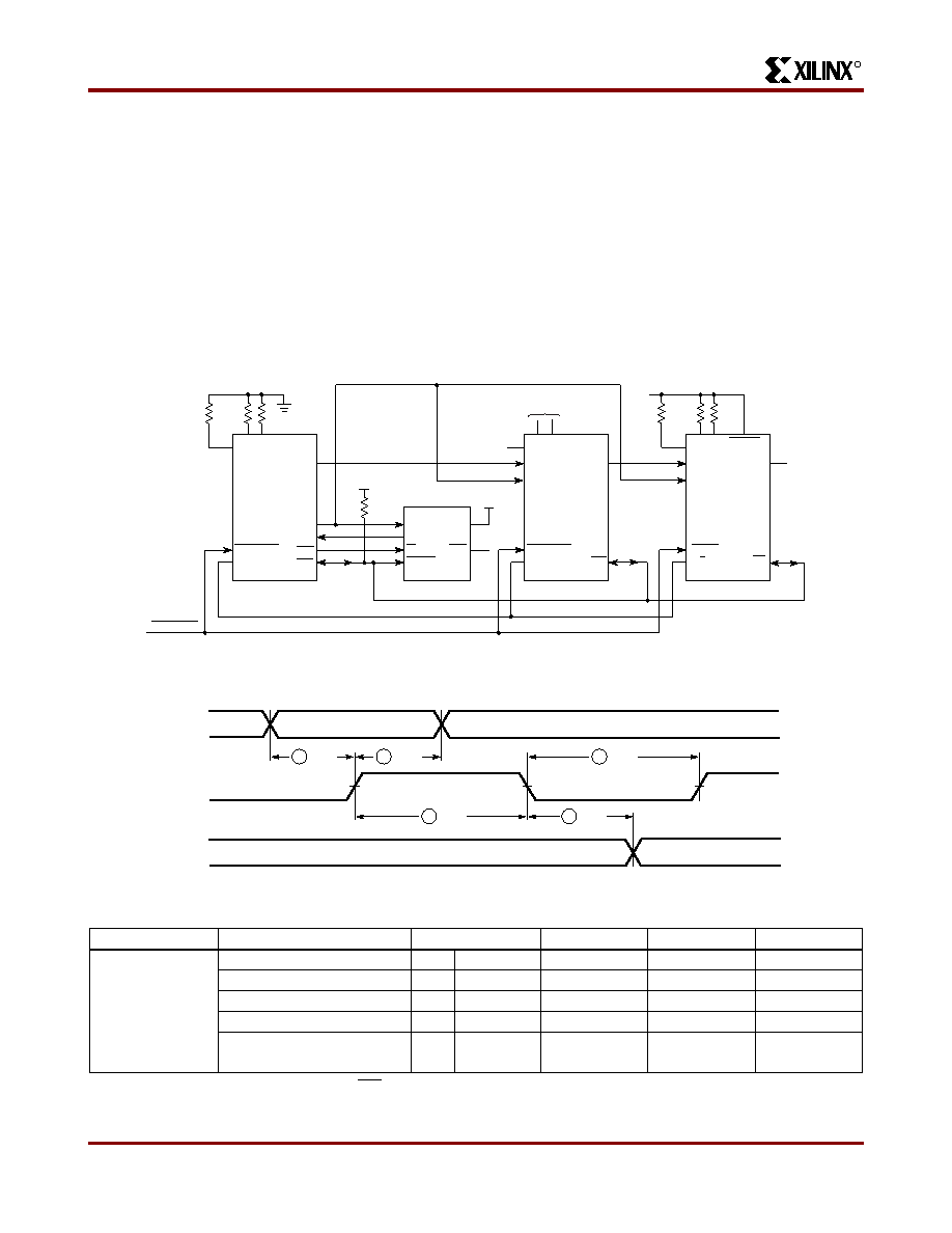
Slave Serial Mode
In Slave Serial mode, an external signal drives the CCLK
input of the FPGA. The serial configuration bitstream must
be available at the DIN input of the lead FPGA a short
setup time before each rising CCLK edge.
The lead FPGA then presents the preamble data—and all
data that overflows the lead device—on its DOUT pin.
There is an internal delay of 0.5 CCLK periods, which
means that DOUT changes on the falling CCLK edge, and
the next FPGA in the daisy chain accepts data on the sub-
sequent rising CCLK edge.
shows
a
full
master/slave
system.
An
XC5200-Series device in Slave Serial mode should be con-
nected as shown in the third device from the left.
Slave Serial mode is selected by a <111> on the mode pins
(M2, M1, M0). Slave Serial is the default mode if the mode
pins are left unconnected, as they have weak pull-up resis-
tors during configuration.
Note:
Configuration must be delayed until the INIT pins of all daisy-chained FPGAs are High.
Figure 29: Slave Serial Mode Programming Switching Characteristics
XC5200
MASTER
SERIAL
Spartan,
XC4000E/EX,
XC5200
SLAVE
XC3100A
SLAVE
XC1700E
PROGRAM
NOTE:
M2, M1, M0 can be shorted
to Ground if not used as I/O
NOTE:
M2, M1, M0 can be shorted
to VCC if not used as I/O
M2
M0 M1
DOUT
CCLK
CLK
VCC
+5 V
DATA
CE
CEO
VPP
RESET/OE
DONE
DIN
LDC
INIT
DONE
PROGRAM
D/P
INIT
RESET
CCLK
DIN
CCLK
DIN
DOUT
M2
M0 M1
M1
PWRDN
M0
M2
(Low Reset Option Used)
4.7 K
3.3 K
3.3 K
3.3 K
3.3 K
3.3 K
3.3 K
VCC
X9003_01
N/C
Figure 28: Master/Slave Serial Mode Circuit Diagram
4 TCCH
Bit n
Bit n + 1
Bit n
Bit n - 1
3 TCCO
5 TCCL
2 TCCD
1 TDCC
DIN
CCLK
DOUT
(Output)
X5379
Description
Symbol
Min
Max
Units
CCLK
DIN setup
1
TDCC
20
ns
DIN hold
2
TCCD
0ns
DIN to DOUT
3
TCCO
30
ns
High time
4
TCCH
45
ns
Low time
5
TCCL
45
ns
Frequency
FCC
10
MHz
相关PDF资料 |
PDF描述 |
|---|---|
| XC5204-6TQ176C | Field Programmable Gate Arrays |
| XC5204-6VQ64C | Field Programmable Gate Arrays |
| XC5204-3TQ144C | Field Programmable Gate Arrays |
| XC5204-3VQ100C | Field Programmable Gate Arrays |
| XC5204-4PC84C | Field Programmable Gate Arrays |
相关代理商/技术参数 |
参数描述 |
|---|---|
| XC5204-6PQG160C | 制造商:Xilinx 功能描述:XC5204-6PQG160C, FPGA XC5200 FAMILY 6K GATES 480 CELLS - Trays 制造商:Xilinx 功能描述:Xilinx XC5204-6PQG160C, FPGA XC5200 Family 6K Gates 480 Cells 83MHz 0.5um (CMOS) Technology 5V 160-Pin PQFP |
| XC5204-6TQ144C | 功能描述:IC FPGA 120 CLB'S 144-TQFP RoHS:否 类别:集成电路 (IC) >> 嵌入式 - FPGA(现场可编程门阵列) 系列:XC5200 产品变化通告:XC4000(E,L) Discontinuation 01/April/2002 标准包装:24 系列:XC4000E/X LAB/CLB数:100 逻辑元件/单元数:238 RAM 位总计:3200 输入/输出数:80 门数:3000 电源电压:4.5 V ~ 5.5 V 安装类型:表面贴装 工作温度:-40°C ~ 100°C 封装/外壳:120-BCBGA 供应商设备封装:120-CPGA(34.55x34.55) |
| XC5204-6TQ144I | 制造商:Xilinx 功能描述: |
| XC5204-6TQ176C | 制造商:XILINX 制造商全称:XILINX 功能描述:Field Programmable Gate Arrays |
| XC5204-6VQ100C | 功能描述:IC FPGA 120 CLB'S 100-VQFP RoHS:否 类别:集成电路 (IC) >> 嵌入式 - FPGA(现场可编程门阵列) 系列:XC5200 产品变化通告:XC4000(E,L) Discontinuation 01/April/2002 标准包装:24 系列:XC4000E/X LAB/CLB数:100 逻辑元件/单元数:238 RAM 位总计:3200 输入/输出数:80 门数:3000 电源电压:4.5 V ~ 5.5 V 安装类型:表面贴装 工作温度:-40°C ~ 100°C 封装/外壳:120-BCBGA 供应商设备封装:120-CPGA(34.55x34.55) |
发布紧急采购,3分钟左右您将得到回复。