- 您现在的位置:买卖IC网 > PDF目录205934 > XC5204-6PQ240C (Xilinx, Inc.) Field Programmable Gate Arrays PDF资料下载
参数资料
| 型号: | XC5204-6PQ240C |
| 厂商: | Xilinx, Inc. |
| 英文描述: | Field Programmable Gate Arrays |
| 中文描述: | 现场可编程门阵列 |
| 文件页数: | 25/73页 |
| 文件大小: | 598K |
| 代理商: | XC5204-6PQ240C |
第1页第2页第3页第4页第5页第6页第7页第8页第9页第10页第11页第12页第13页第14页第15页第16页第17页第18页第19页第20页第21页第22页第23页第24页当前第25页第26页第27页第28页第29页第30页第31页第32页第33页第34页第35页第36页第37页第38页第39页第40页第41页第42页第43页第44页第45页第46页第47页第48页第49页第50页第51页第52页第53页第54页第55页第56页第57页第58页第59页第60页第61页第62页第63页第64页第65页第66页第67页第68页第69页第70页第71页第72页第73页
R
November 5, 1998 (Version 5.2)
7-113
XC5200 Series Field Programmable Gate Arrays
7
Note that in XC5200-Series devices, configuration data is
not inverted with respect to configuration as it is in XC2000
and XC3000 families.
Readback of Express mode bitstreams results in data that
does not resemble the original bitstream, because the bit-
stream format differs from other modes.
XC5200-Series Readback does not use any dedicated
pins,
but
uses
four
internal
nets
(RDBK.TRIG,
RDBK.DATA, RDBK.RIP and RDBK.CLK) that can be
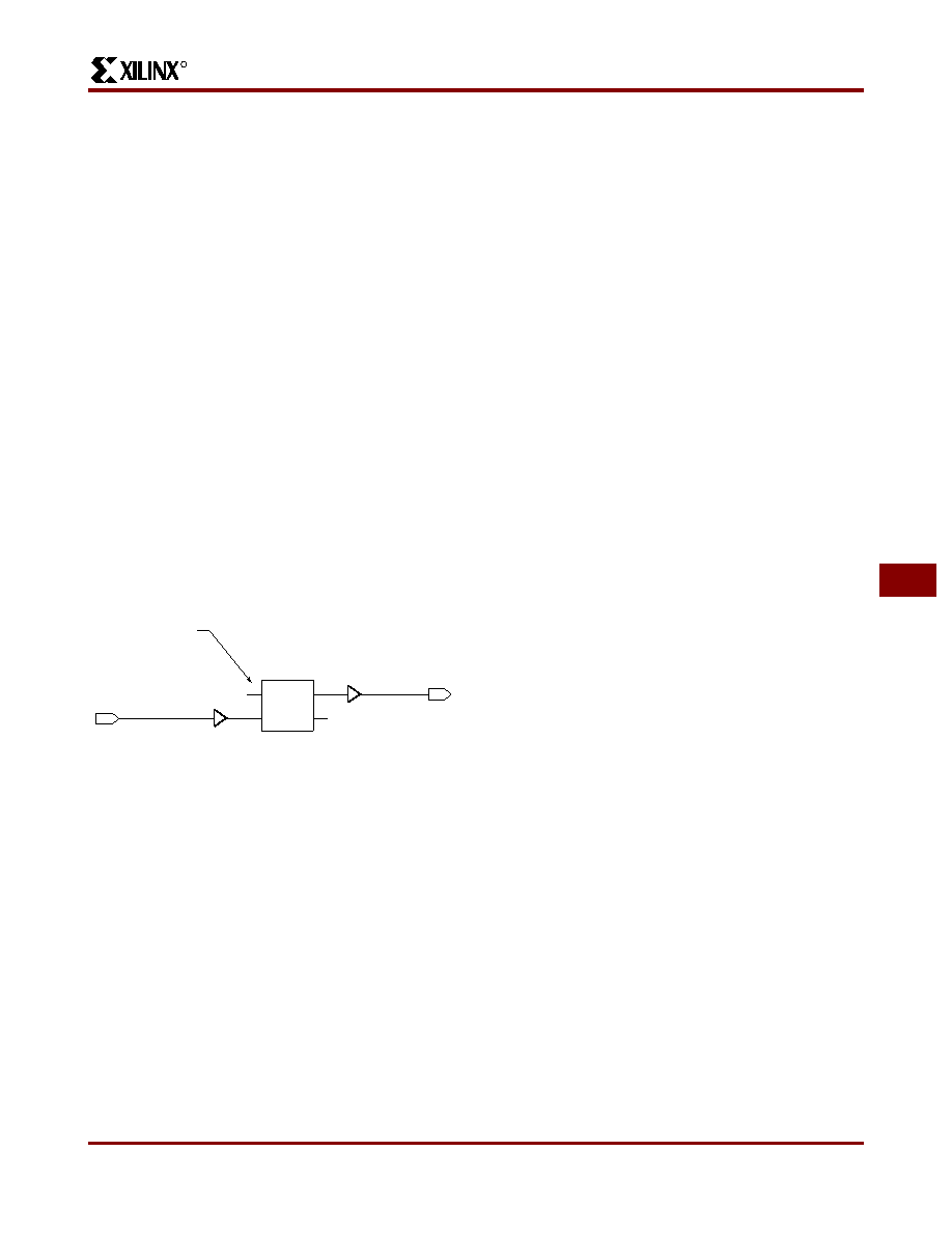
routed to any IOB. To access the internal Readback sig-
nals, place the READBACK library symbol and attach the
appropriate pad symbols, as shown in Figure 27.
After Readback has been initiated by a Low-to-High transi-
tion on RDBK.TRIG, the RDBK.RIP (Read In Progress)
output goes High on the next rising edge of RDBK.CLK.
Subsequent rising edges of this clock shift out Readback
data on the RDBK.DATA net.
Readback data does not include the preamble, but starts
with five dummy bits (all High) followed by the Start bit
(Low) of the first frame. The first two data bits of the first
frame are always High.
Each frame ends with four error check bits. They are read
back as High. The last seven bits of the last frame are also
read back as High. An additional Start bit (Low) and an
11-bit Cyclic Redundancy Check (CRC) signature follow,
before RDBK.RIP returns Low.
Readback Options
Readback options are: Read Capture, Read Abort, and
Clock Select. They are set with the bitstream generation
software.
Read Capture
When the Read Capture option is selected, the readback
data stream includes sampled values of CLB and IOB sig-
nals. The rising edge of RDBK.TRIG latches the inverted
values of the CLB outputs and the IOB output and input sig-
nals.
Note that while the bits describing configuration
(interconnect and function generators) are
not inverted, the
CLB and IOB output signals
are inverted.
When the Read Capture option is not selected, the values
of the capture bits reflect the configuration data originally
written to those memory locations.
The readback signals are located in the lower-left corner of
the device.
Read Abort
When the Read Abort option is selected, a High-to-Low
transition on RDBK.TRIG terminates the readback opera-
tion and prepares the logic to accept another trigger.
After an aborted readback, additional clocks (up to one
readback clock per configuration frame) may be required to
re-initialize the control logic. The status of readback is indi-
cated by the output control net RDBK.RIP. RDBK.RIP is
High whenever a readback is in progress.
Clock Select
CCLK is the default clock. However, the user can insert
another clock on RDBK.CLK. Readback control and data
are clocked on rising edges of RDBK.CLK. If readback
must be inhibited for security reasons, the readback control
nets are simply not connected.
Violating the Maximum High and Low Time
Specification for the Readback Clock
The readback clock has a maximum High and Low time
specification. In some cases, this specification cannot be
met. For example, if a processor is controlling readback,
an interrupt may force it to stop in the middle of a readback.
This necessitates stopping the clock, and thus violating the
specification.
The specification is mandatory only on clocking data at the
end of a frame prior to the next start bit. The transfer mech-
anism will load the data to a shift register during the last six
clock cycles of the frame, prior to the start bit of the follow-
ing frame. This loading process is dynamic, and is the
source of the maximum High and Low time requirements.
Therefore, the specification only applies to the six clock
cycles prior to and including any start bit, including the
clocks before the first start bit in the readback data stream.
At other times, the frame data is already in the register and
the register is not dynamic. Thus, it can be shifted out just
like a regular shift register.
The user must precisely calculate the location of the read-
back data relative to the frame. The system must keep
track of the position within a data frame, and disable inter-
rupts before frame boundaries. Frame lengths and data for-
Readback with the XChecker Cable
The XChecker Universal Download/Readback Cable and
Logic Probe uses the readback feature for bitstream verifi-
cation. It can also display selected internal signals on the
PC or workstation screen, functioning as a low-cost in-cir-
cuit emulator.
READBACK
DATA
RIP
TRIG
CLK
READ_DATA
OBUF
MD1
MD0
READ_TRIGGER
IBUF
X1786
IF UNCONNECTED,
DEFAULT IS CCLK
Figure 27: Readback Schematic Example
相关PDF资料 |
PDF描述 |
|---|---|
| XC5204-6TQ176C | Field Programmable Gate Arrays |
| XC5204-6VQ64C | Field Programmable Gate Arrays |
| XC5204-3TQ144C | Field Programmable Gate Arrays |
| XC5204-3VQ100C | Field Programmable Gate Arrays |
| XC5204-4PC84C | Field Programmable Gate Arrays |
相关代理商/技术参数 |
参数描述 |
|---|---|
| XC5204-6PQG160C | 制造商:Xilinx 功能描述:XC5204-6PQG160C, FPGA XC5200 FAMILY 6K GATES 480 CELLS - Trays 制造商:Xilinx 功能描述:Xilinx XC5204-6PQG160C, FPGA XC5200 Family 6K Gates 480 Cells 83MHz 0.5um (CMOS) Technology 5V 160-Pin PQFP |
| XC5204-6TQ144C | 功能描述:IC FPGA 120 CLB'S 144-TQFP RoHS:否 类别:集成电路 (IC) >> 嵌入式 - FPGA(现场可编程门阵列) 系列:XC5200 产品变化通告:XC4000(E,L) Discontinuation 01/April/2002 标准包装:24 系列:XC4000E/X LAB/CLB数:100 逻辑元件/单元数:238 RAM 位总计:3200 输入/输出数:80 门数:3000 电源电压:4.5 V ~ 5.5 V 安装类型:表面贴装 工作温度:-40°C ~ 100°C 封装/外壳:120-BCBGA 供应商设备封装:120-CPGA(34.55x34.55) |
| XC5204-6TQ144I | 制造商:Xilinx 功能描述: |
| XC5204-6TQ176C | 制造商:XILINX 制造商全称:XILINX 功能描述:Field Programmable Gate Arrays |
| XC5204-6VQ100C | 功能描述:IC FPGA 120 CLB'S 100-VQFP RoHS:否 类别:集成电路 (IC) >> 嵌入式 - FPGA(现场可编程门阵列) 系列:XC5200 产品变化通告:XC4000(E,L) Discontinuation 01/April/2002 标准包装:24 系列:XC4000E/X LAB/CLB数:100 逻辑元件/单元数:238 RAM 位总计:3200 输入/输出数:80 门数:3000 电源电压:4.5 V ~ 5.5 V 安装类型:表面贴装 工作温度:-40°C ~ 100°C 封装/外壳:120-BCBGA 供应商设备封装:120-CPGA(34.55x34.55) |
发布紧急采购,3分钟左右您将得到回复。