- 您现在的位置:买卖IC网 > PDF目录205934 > XC5204-6PQ240C (Xilinx, Inc.) Field Programmable Gate Arrays PDF资料下载
参数资料
| 型号: | XC5204-6PQ240C |
| 厂商: | Xilinx, Inc. |
| 英文描述: | Field Programmable Gate Arrays |
| 中文描述: | 现场可编程门阵列 |
| 文件页数: | 19/73页 |
| 文件大小: | 598K |
| 代理商: | XC5204-6PQ240C |
第1页第2页第3页第4页第5页第6页第7页第8页第9页第10页第11页第12页第13页第14页第15页第16页第17页第18页当前第19页第20页第21页第22页第23页第24页第25页第26页第27页第28页第29页第30页第31页第32页第33页第34页第35页第36页第37页第38页第39页第40页第41页第42页第43页第44页第45页第46页第47页第48页第49页第50页第51页第52页第53页第54页第55页第56页第57页第58页第59页第60页第61页第62页第63页第64页第65页第66页第67页第68页第69页第70页第71页第72页第73页
R
XC5200 Series Field Programmable Gate Arrays
7-108
November 5, 1998 (Version 5.2)
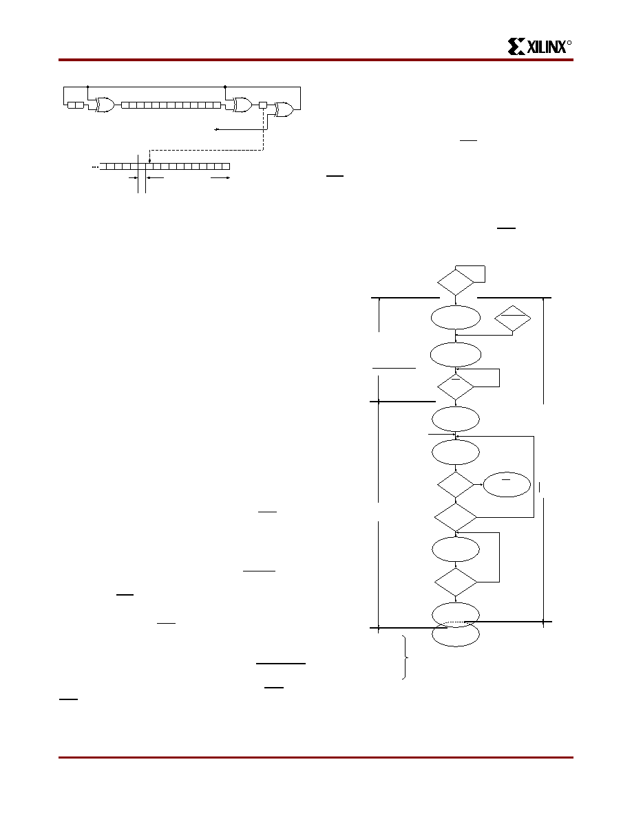
Configuration Sequence
There are four major steps in the XC5200-Series power-up
configuration sequence.
Power-On Time-Out
Initialization
Configuration
Start-Up
The full process is illustrated in Figure 24.
Power-On Time-Out
An internal power-on reset circuit is triggered when power
is applied. When V
CC reaches the voltage at which portions
of
the
FPGA
begin
to
operate
(i.e.,
performs
a
write-and-read test of a sample pair of configuration mem-
ory bits), the programmable I/O buffers are 3-stated with
active high-impedance pull-up resistors. A time-out delay
— nominally 4 ms — is initiated to allow the power-supply
voltage to stabilize. For correct operation the power supply
must reach V
CC(min) by the end of the time-out, and must
not dip below it thereafter.
There is no distinction between master and slave modes
with regard to the time-out delay. Instead, the INIT line is
used to ensure that all daisy-chained devices have com-
pleted initialization. Since XC2000 devices do not have this
signal, extra care must be taken to guarantee proper oper-
ation when daisy-chaining them with XC5200 devices. For
proper operation with XC3000 devices, the RESET signal,
which is used in XC3000 to delay configuration, should be
connected to INIT.
If the time-out delay is insufficient, configuration should be
delayed by holding the INIT pin Low until the power supply
has reached operating levels.
This delay is applied only on power-up. It is not applied
when reconfiguring an FPGA by pulsing the PROGRAM
pin Low. During all three phases — Power-on, Initialization,
and Configuration — DONE is held Low; HDC, LDC, and
INIT are active; DOUT is driven; and all I/O buffers are dis-
abled.
Initialization
This phase clears the configuration memory and estab-
lishes the configuration mode.
The configuration memory is cleared at the rate of one
frame per internal clock cycle (nominally 1 MHz). An
open-drain bidirectional signal, INIT, is released when the
configuration memory is completely cleared. The device
then tests for the absence of an external active-low level on
INIT. The mode lines are sampled two internal clock cycles
later (nominally 2
s).
The master device waits an additional 32
s to 256 s
(nominally 64-128
s) to provide adequate time for all of the
slave devices to recognize the release of INIT as well. Then
the master device enters the Configuration phase.
0
X2
2
3456789 10 11 12 13 14
1
X15
X16
15
SERIAL DATA IN
1
0 1514 13 12 1110 9
8
7
65
1
CRC – CHECKSUM
LAST DATA FRAME
START
BIT
X1789
Polynomial: X16 + X15 + X2 + 1
Readback Data Stream
Figure 23: Circuit for Generating CRC-16
Figure 24: Configuration Sequence
INIT
High? if
Master
Sample
Mode Lines
Load One
Configuration
Data Frame
Frame
Error
Pass
Configuration
Data to DOUT
VCC
3V
No
Yes
No
Yes
Operational
Start-Up
Sequence
No
Yes
~1.3
s per Frame
Master CCLK
Goes Active after
50 to 250
s
F
Pull INIT Low
and Stop
X9017
EXTEST*
SAMPLE/PRELOAD*
BYPASS
CONFIGURE*
(*only when PROGRAM = High)
SAMPLE/PRELOAD
BYPASS
EXTEST
SAMPLE PRELOAD
BYPASS
USER 1
USER 2
CONFIGURE
READBACK
If Boundary Scan
is Selected
Config-
uration
memory
Full
CCLK
Count Equals
Length
Count
Completely Clear
Configuration
Memory
LDC
Output
=
L,
HDC
Output
=
H
Boundary Scan
Instructions
Available:
I/O
Active
Generate
One Time-Out Pulse
of 4 ms
PROGRAM
= Low
No
Yes
相关PDF资料 |
PDF描述 |
|---|---|
| XC5204-6TQ176C | Field Programmable Gate Arrays |
| XC5204-6VQ64C | Field Programmable Gate Arrays |
| XC5204-3TQ144C | Field Programmable Gate Arrays |
| XC5204-3VQ100C | Field Programmable Gate Arrays |
| XC5204-4PC84C | Field Programmable Gate Arrays |
相关代理商/技术参数 |
参数描述 |
|---|---|
| XC5204-6PQG160C | 制造商:Xilinx 功能描述:XC5204-6PQG160C, FPGA XC5200 FAMILY 6K GATES 480 CELLS - Trays 制造商:Xilinx 功能描述:Xilinx XC5204-6PQG160C, FPGA XC5200 Family 6K Gates 480 Cells 83MHz 0.5um (CMOS) Technology 5V 160-Pin PQFP |
| XC5204-6TQ144C | 功能描述:IC FPGA 120 CLB'S 144-TQFP RoHS:否 类别:集成电路 (IC) >> 嵌入式 - FPGA(现场可编程门阵列) 系列:XC5200 产品变化通告:XC4000(E,L) Discontinuation 01/April/2002 标准包装:24 系列:XC4000E/X LAB/CLB数:100 逻辑元件/单元数:238 RAM 位总计:3200 输入/输出数:80 门数:3000 电源电压:4.5 V ~ 5.5 V 安装类型:表面贴装 工作温度:-40°C ~ 100°C 封装/外壳:120-BCBGA 供应商设备封装:120-CPGA(34.55x34.55) |
| XC5204-6TQ144I | 制造商:Xilinx 功能描述: |
| XC5204-6TQ176C | 制造商:XILINX 制造商全称:XILINX 功能描述:Field Programmable Gate Arrays |
| XC5204-6VQ100C | 功能描述:IC FPGA 120 CLB'S 100-VQFP RoHS:否 类别:集成电路 (IC) >> 嵌入式 - FPGA(现场可编程门阵列) 系列:XC5200 产品变化通告:XC4000(E,L) Discontinuation 01/April/2002 标准包装:24 系列:XC4000E/X LAB/CLB数:100 逻辑元件/单元数:238 RAM 位总计:3200 输入/输出数:80 门数:3000 电源电压:4.5 V ~ 5.5 V 安装类型:表面贴装 工作温度:-40°C ~ 100°C 封装/外壳:120-BCBGA 供应商设备封装:120-CPGA(34.55x34.55) |
发布紧急采购,3分钟左右您将得到回复。