- 您现在的位置:买卖IC网 > PDF目录205934 > XC5204-6PQ240C (Xilinx, Inc.) Field Programmable Gate Arrays PDF资料下载
参数资料
| 型号: | XC5204-6PQ240C |
| 厂商: | Xilinx, Inc. |
| 英文描述: | Field Programmable Gate Arrays |
| 中文描述: | 现场可编程门阵列 |
| 文件页数: | 40/73页 |
| 文件大小: | 598K |
| 代理商: | XC5204-6PQ240C |
第1页第2页第3页第4页第5页第6页第7页第8页第9页第10页第11页第12页第13页第14页第15页第16页第17页第18页第19页第20页第21页第22页第23页第24页第25页第26页第27页第28页第29页第30页第31页第32页第33页第34页第35页第36页第37页第38页第39页当前第40页第41页第42页第43页第44页第45页第46页第47页第48页第49页第50页第51页第52页第53页第54页第55页第56页第57页第58页第59页第60页第61页第62页第63页第64页第65页第66页第67页第68页第69页第70页第71页第72页第73页
R
November 5, 1998 (Version 5.2)
7-127
XC5200 Series Field Programmable Gate Arrays
7
XC5200 Switching Characteristics
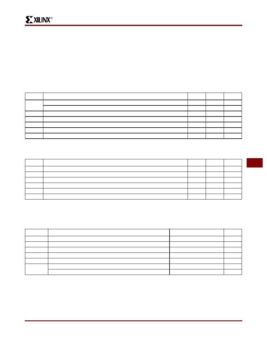
Definition of Terms
In the following tables, some specifications may be designated as Advance or Preliminary. These terms are defined as
follows:
Advance:
Initial estimates based on simulation and/or extrapolation from other speed grades, devices, or device
families. Use as estimates, not for production.
Preliminary: Based on preliminary characterization. Further changes are not expected.
Unmarked:
Specifications not identified as either Advance or Preliminary are to be considered Final.1
XC5200 Operating Conditions
XC5200 DC Characteristics Over Operating Conditions
XC5200 Absolute Maximum Ratings
1. Notwithstanding the definition of the above terms, all specifications are subject to change without notice.
Symbol
Description
Min
Max
Units
V
CC
Supply voltage relative to GND Commercial: 0
°C to 85°C junction
4.75
5.25
V
Supply voltage relative to GND Industrial: -40
°C to 100°C junction
4.5
5.5
V
IHT
High-level input voltage — TTL configuration
2.0
V
CC
V
ILT
Low-level input voltage — TTL configuration
0
0.8
V
IHC
High-level input voltage — CMOS configuration
70%
100%
V
CC
V
ILC
Low-level input voltage — CMOS configuration
0
20%
V
CC
T
IN
Input signal transition time
250
ns
Symbol
Description
Min
Max
Units
V
OH
High-level output voltage @ I
OH = -8.0 mA, VCC min
3.86
V
OL
Low-level output voltage @ I
OL = 8.0 mA, VCC max
0.4
V
I
CCO
Quiescent FPGA supply current (Note 1)
15
mA
I
IL
Leakage current
-10
+10
A
C
IN
Input capacitance (sample tested)
15
pF
I
RIN
Pad pull-up (when selected) @ V
IN = 0V (sample tested)
0.02
0.30
mA
Note:
1. With no output current loads, all package pins at Vcc or GND, either TTL or CMOS inputs, and the FPGA configured with a
tie option.
Symbol
Description
Units
V
CC
Supply voltage relative to GND
-0.5 to +7.0
V
IN
Input voltage with respect to GND
-0.5 to V
CC +0.5
V
TS
Voltage applied to 3-state output
-0.5 to V
CC +0.5
V
T
STG
Storage temperature (ambient)
-65 to +150
°C
T
SOL
Maximum soldering temperature (10 s @ 1/16 in. = 1.5 mm)
+260
°C
T
J
Junction temperature in plastic packages
+125
°C
Junction temperature in ceramic packages
+150
°C
Note: Stresses beyond those listed under Absolute Maximum Ratings may cause permanent damage to the device. These are stress
ratings only, and functional operation of the device at these or any other conditions beyond those listed under Recommended
Operating Conditions is not implied. Exposure to Absolute Maximum Ratings conditions for extended periods of time may
affect device reliability.
相关PDF资料 |
PDF描述 |
|---|---|
| XC5204-6TQ176C | Field Programmable Gate Arrays |
| XC5204-6VQ64C | Field Programmable Gate Arrays |
| XC5204-3TQ144C | Field Programmable Gate Arrays |
| XC5204-3VQ100C | Field Programmable Gate Arrays |
| XC5204-4PC84C | Field Programmable Gate Arrays |
相关代理商/技术参数 |
参数描述 |
|---|---|
| XC5204-6PQG160C | 制造商:Xilinx 功能描述:XC5204-6PQG160C, FPGA XC5200 FAMILY 6K GATES 480 CELLS - Trays 制造商:Xilinx 功能描述:Xilinx XC5204-6PQG160C, FPGA XC5200 Family 6K Gates 480 Cells 83MHz 0.5um (CMOS) Technology 5V 160-Pin PQFP |
| XC5204-6TQ144C | 功能描述:IC FPGA 120 CLB'S 144-TQFP RoHS:否 类别:集成电路 (IC) >> 嵌入式 - FPGA(现场可编程门阵列) 系列:XC5200 产品变化通告:XC4000(E,L) Discontinuation 01/April/2002 标准包装:24 系列:XC4000E/X LAB/CLB数:100 逻辑元件/单元数:238 RAM 位总计:3200 输入/输出数:80 门数:3000 电源电压:4.5 V ~ 5.5 V 安装类型:表面贴装 工作温度:-40°C ~ 100°C 封装/外壳:120-BCBGA 供应商设备封装:120-CPGA(34.55x34.55) |
| XC5204-6TQ144I | 制造商:Xilinx 功能描述: |
| XC5204-6TQ176C | 制造商:XILINX 制造商全称:XILINX 功能描述:Field Programmable Gate Arrays |
| XC5204-6VQ100C | 功能描述:IC FPGA 120 CLB'S 100-VQFP RoHS:否 类别:集成电路 (IC) >> 嵌入式 - FPGA(现场可编程门阵列) 系列:XC5200 产品变化通告:XC4000(E,L) Discontinuation 01/April/2002 标准包装:24 系列:XC4000E/X LAB/CLB数:100 逻辑元件/单元数:238 RAM 位总计:3200 输入/输出数:80 门数:3000 电源电压:4.5 V ~ 5.5 V 安装类型:表面贴装 工作温度:-40°C ~ 100°C 封装/外壳:120-BCBGA 供应商设备封装:120-CPGA(34.55x34.55) |
发布紧急采购,3分钟左右您将得到回复。