参数资料
| 型号: | XC6VCX195T-2FFG784I |
| 厂商: | Xilinx Inc |
| 文件页数: | 22/52页 |
| 文件大小: | 0K |
| 描述: | IC FPGA VIRTEX 6 199K 784FFGBGA |
| 产品培训模块: | Virtex-6 FPGA Overview |
| 产品变化通告: | Virtex-6 FIFO Input Logic Reset 18/Apr/2011 |
| 标准包装: | 1 |
| 系列: | Virtex® 6 CXT |
| LAB/CLB数: | 15600 |
| 逻辑元件/单元数: | 199680 |
| RAM 位总计: | 12681216 |
| 输入/输出数: | 400 |
| 电源电压: | 0.95 V ~ 1.05 V |
| 安装类型: | 表面贴装 |
| 工作温度: | -40°C ~ 100°C |
| 封装/外壳: | 784-BBGA,FCBGA |
| 供应商设备封装: | 784-FCBGA |
第1页第2页第3页第4页第5页第6页第7页第8页第9页第10页第11页第12页第13页第14页第15页第16页第17页第18页第19页第20页第21页当前第22页第23页第24页第25页第26页第27页第28页第29页第30页第31页第32页第33页第34页第35页第36页第37页第38页第39页第40页第41页第42页第43页第44页第45页第46页第47页第48页第49页第50页第51页第52页
Virtex-6 CXT Family Data Sheet
DS153 (v1.6) February 11, 2011
Product Specification
29
I/O Standard Adjustment Measurement Methodology
Input Delay Measurements
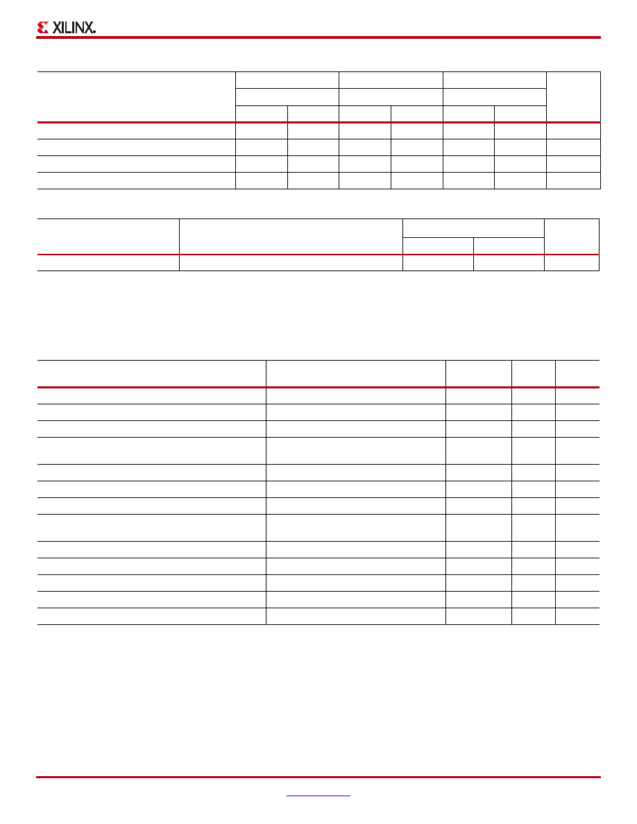
Table 40 shows the test setup parameters used for measuring input delay.
DIFF_SSTL18_II_T_DCI
1.09
1.67
ns
DIFF_SSTL15
1.06
1.71
ns
DIFF_SSTL15_DCI
1.06
1.68
ns
DIFF_SSTL15_T_DCI
1.06
1.68
ns
Table 39: IOB 3-state ON Output Switching Characteristics (TIOTPHZ)
Symbol
Description
Speed Grade
Units
-2
-1
TIOTPHZ
T input to Pad high-impedance
0.99
ns
Table 38: IOB Switching Characteristics (Cont’d)
I/O Standard
TIOPI
TIOOP
TIOTP
Units
Speed Grade
-2
-1
-2
-1
-2
-1
Table 40: Input Delay Measurement Methodology
Description
I
/O Standard Attribute
VL(1)(2)
VH(1)(2)
VMEAS
(1,4,5)
VREF
(1,3,5)
LVCMOS, 2.5V
LVCMOS25
0
2.5
1.25
–
LVCMOS, 1.8V
LVCMOS18
0
1.8
0.9
–
LVCMOS, 1.5V
LVCMOS15
0
1.5
0.75
–
HSTL (High-Speed Transceiver Logic),
Class I & II
HSTL_I, HSTL_II
VREF –0.5
VREF +0.5
VREF
0.75
HSTL, Class III
HSTL_III
VREF –0.5
VREF +0.5
VREF
0.90
HSTL, Class I & II, 1.8V
HSTL_I_18, HSTL_II_18
VREF –0.5
VREF +0.5
VREF
0.90
HSTL, Class III 1.8V
HSTL_III_18
VREF –0.5
VREF +0.5
VREF
1.08
SSTL (Stub Terminated Transceiver Logic),
Class I & II, 3.3V
SSTL3_I, SSTL3_II
VREF –1.00
VREF +1.00
VREF
1.5
SSTL, Class I & II, 2.5V
SSTL2_I, SSTL2_II
VREF –0.75
VREF +0.75
VREF
1.25
SSTL, Class I & II, 1.8V
SSTL18_I, SSTL18_II
VREF –0.5
VREF +0.5
VREF
0.90
LVDS (Low-Voltage Differential Signaling), 2.5V
LVDS_25
1.2 – 0.125
1.2 + 0.125
–
LVDSEXT (LVDS Extended Mode), 2.5V
LVDSEXT_25
1.2 – 0.125
1.2 + 0.125
–
HT (HyperTransport), 2.5V
LDT_25
0.6 – 0.125
0.6 + 0.125
–
Notes:
1.
The input delay measurement methodology parameters for LVDCI are the same for LVCMOS standards of the same voltage. Input delay
measurement methodology parameters for HSLVDCI are the same as for HSTL_II standards of the same voltage. Parameters for all other
DCI standards are the same for the corresponding non-DCI standards.
2.
Input waveform switches between VLand VH.
3.
Measurements are made at typical, minimum, and maximum VREF values. Reported delays reflect worst case of these measurements. VREF
values listed are typical.
4.
Input voltage level from which measurement starts.
5.
This is an input voltage reference that bears no relation to the VREF / VMEAS parameters found in IBIS models and/or noted in Figure 14.
6.
The value given is the differential output voltage.
相关PDF资料 |
PDF描述 |
|---|---|
| ABB106DHFN-S578 | EDGECARD 212POS .050 SMD W/POSTS |
| XC5VLX110-1FFG1760C | IC FPGA VIRTEX-5 110K 1760FBGA |
| ACB106DHFD-S578 | EDGECARD 212POS .050 SMD W/POSTS |
| ABB106DHFD-S578 | EDGECARD 212POS .050 SMD W/POSTS |
| XC5VLX110-1FFG1153C | IC FPGA VIRTEX-5 110K 1153FBGA |
相关代理商/技术参数 |
参数描述 |
|---|---|
| XC6VCX240T | 制造商:XILINX 制造商全称:XILINX 功能描述:Virtex-6 CXT Family Data Sheet |
| XC6VCX240T-1FF1156C | 制造商:Xilinx 功能描述:FPGA VIRTEX?-6 CXT FAMILY 241152 CELLS 40NM (CMOS) TECHNOLOG - Trays 制造商:Xilinx 功能描述:IC FPGA 600 I/O 1156FCBGA |
| XC6VCX240T-1FF1156I | 制造商:Xilinx 功能描述:FPGA VIRTEX?-6 CXT FAMILY 241152 CELLS 40NM (CMOS) TECHNOLOG - Trays 制造商:Xilinx 功能描述:IC FPGA VIRTEX 6 240K 1156BGA 制造商:Xilinx 功能描述:IC FPGA 600 I/O 1156FCBGA |
| XC6VCX240T-1FF784C | 制造商:Xilinx 功能描述:FPGA VIRTEX?-6 CXT FAMILY 241152 CELLS 40NM (CMOS) TECHNOLOG - Trays 制造商:Xilinx 功能描述:IC FPGA VIRTEX 6 240K 784BGA |
| XC6VCX240T-1FF784I | 制造商:Xilinx 功能描述:FPGA VIRTEX?-6 CXT FAMILY 241152 CELLS 40NM (CMOS) TECHNOLOG - Trays 制造商:Xilinx 功能描述:IC FPGA 400 I/O 784FCBGA |
发布紧急采购,3分钟左右您将得到回复。