参数资料
| 型号: | XC6VCX195T-2FFG784I |
| 厂商: | Xilinx Inc |
| 文件页数: | 41/52页 |
| 文件大小: | 0K |
| 描述: | IC FPGA VIRTEX 6 199K 784FFGBGA |
| 产品培训模块: | Virtex-6 FPGA Overview |
| 产品变化通告: | Virtex-6 FIFO Input Logic Reset 18/Apr/2011 |
| 标准包装: | 1 |
| 系列: | Virtex® 6 CXT |
| LAB/CLB数: | 15600 |
| 逻辑元件/单元数: | 199680 |
| RAM 位总计: | 12681216 |
| 输入/输出数: | 400 |
| 电源电压: | 0.95 V ~ 1.05 V |
| 安装类型: | 表面贴装 |
| 工作温度: | -40°C ~ 100°C |
| 封装/外壳: | 784-BBGA,FCBGA |
| 供应商设备封装: | 784-FCBGA |
第1页第2页第3页第4页第5页第6页第7页第8页第9页第10页第11页第12页第13页第14页第15页第16页第17页第18页第19页第20页第21页第22页第23页第24页第25页第26页第27页第28页第29页第30页第31页第32页第33页第34页第35页第36页第37页第38页第39页第40页当前第41页第42页第43页第44页第45页第46页第47页第48页第49页第50页第51页第52页
Virtex-6 CXT Family Data Sheet
DS153 (v1.6) February 11, 2011
Product Specification
46
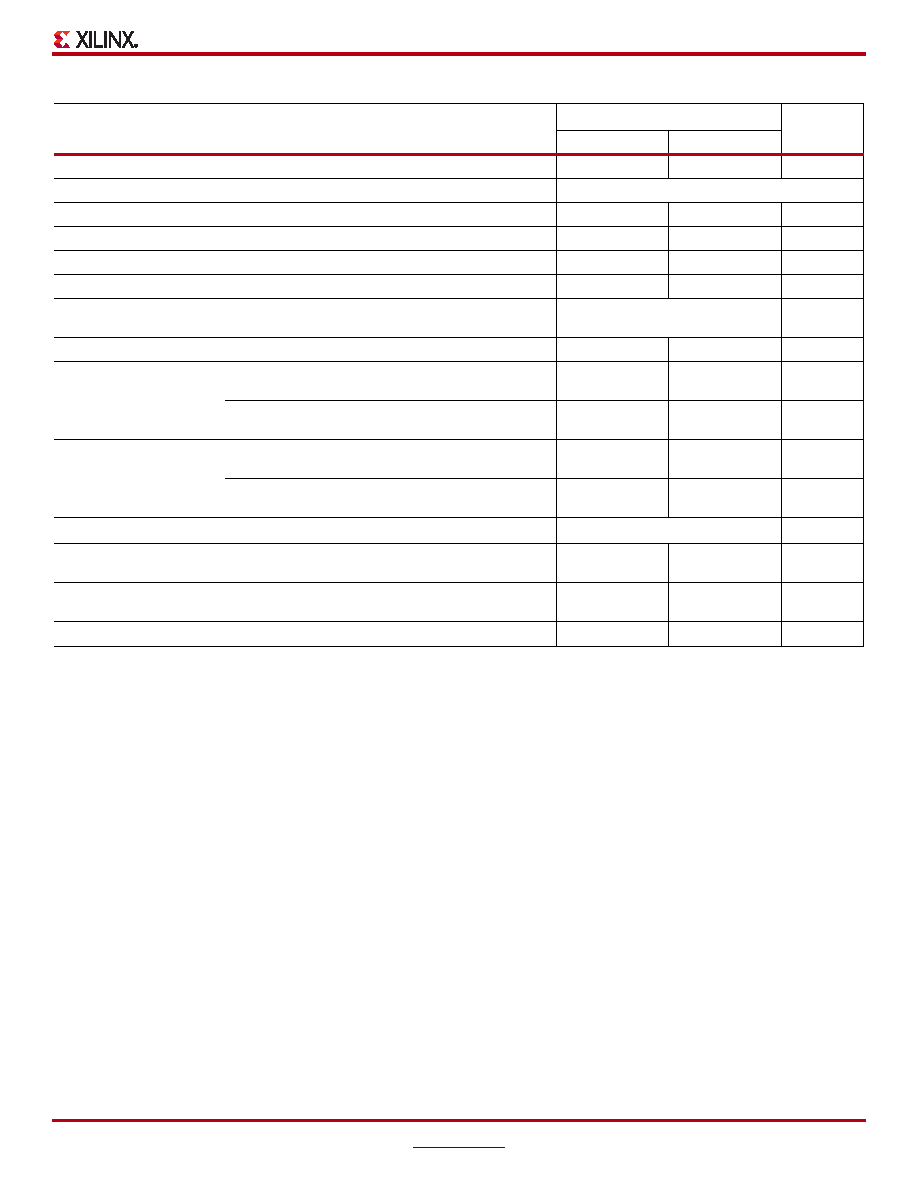
TSTATPHAOFFSET
Static Phase Offset of the MMCM Outputs(3)
0.12
ns
TOUTJITTER
MMCM Output Jitter(4)
Note 1
TOUTDUTY
MMCM Output Clock Duty Cycle Precision(5)
0.20
ns
TLOCKMAX
MMCM Maximum Lock Time
100
s
FOUTMAX
MMCM Maximum Output Frequency
700
MHz
FOUTMIN
MMCM Minimum Output Frequency(6)(7)
4.69
MHz
TEXTFDVAR
External Clock Feedback Variation
< 20% of clock input period or 1 ns
Max
RSTMINPULSE
Minimum Reset Pulse Width
1.5
ns
FPFDMAX
Maximum Frequency at the Phase Frequency Detector
with Bandwidth Set to High or Optimized(8)
450
MHz
Maximum Frequency at the Phase Frequency Detector
with Bandwidth Set to Low
300
MHz
FPFDMIN
Minimum Frequency at the Phase Frequency Detector
with Bandwidth Set to High or Optimized
135
MHz
Minimum Frequency at the Phase Frequency Detector
with Bandwidth Set to Low
10.00
MHz
TFBDELAY
Maximum Delay in the Feedback Path
3 ns Max or one CLKIN cycle
TMMCMDCK_PSEN/
TMMCMCKD_PSEN
Setup and Hold of Phase Shift Enable
1.04/0.00
ns
TMMCMDCK_PSINCDEC/
TMMCMCKD_PSINCDEC
Setup and Hold of Phase Shift Increment/Decrement
1.04/0.00
ns
TMMCMCKO_PSDONE
Phase Shift Clock-to-Out of PSDONE
0.38
ns
Notes:
1.
When DIVCLK_DIVIDE = 3 or 4, FINMAX is 315 MHz.
2.
The MMCM does not filter typical spread-spectrum input clocks because they are usually far below the bandwidth filter frequencies.
3.
The static offset is measured between any MMCM outputs with identical phase.
4.
Values for this parameter are available in the Architecture Wizard.
5.
Includes global clock buffer.
6.
Calculated as FVCO/128 assuming output duty cycle is 50%.
7.
When CASCADE4_OUT = TRUE, FOUTMIN is 0.036 MHz.
8.
In ISE software 12.3 (or earlier versions supporting the Virtex-6 family), the phase frequency detector Optimized bandwidth setting is
equivalent to the High bandwidth setting. Starting with ISE software 12.4, the Optimized bandwidth setting is automatically adjusted to Low
when the software can determine that the phase frequency detector input is less than 135 MHz.
Table 57: MMCM Specification (Cont’d)
Symbol
Description
Speed Grade
Units
-2
-1
相关PDF资料 |
PDF描述 |
|---|---|
| ABB106DHFN-S578 | EDGECARD 212POS .050 SMD W/POSTS |
| XC5VLX110-1FFG1760C | IC FPGA VIRTEX-5 110K 1760FBGA |
| ACB106DHFD-S578 | EDGECARD 212POS .050 SMD W/POSTS |
| ABB106DHFD-S578 | EDGECARD 212POS .050 SMD W/POSTS |
| XC5VLX110-1FFG1153C | IC FPGA VIRTEX-5 110K 1153FBGA |
相关代理商/技术参数 |
参数描述 |
|---|---|
| XC6VCX240T | 制造商:XILINX 制造商全称:XILINX 功能描述:Virtex-6 CXT Family Data Sheet |
| XC6VCX240T-1FF1156C | 制造商:Xilinx 功能描述:FPGA VIRTEX?-6 CXT FAMILY 241152 CELLS 40NM (CMOS) TECHNOLOG - Trays 制造商:Xilinx 功能描述:IC FPGA 600 I/O 1156FCBGA |
| XC6VCX240T-1FF1156I | 制造商:Xilinx 功能描述:FPGA VIRTEX?-6 CXT FAMILY 241152 CELLS 40NM (CMOS) TECHNOLOG - Trays 制造商:Xilinx 功能描述:IC FPGA VIRTEX 6 240K 1156BGA 制造商:Xilinx 功能描述:IC FPGA 600 I/O 1156FCBGA |
| XC6VCX240T-1FF784C | 制造商:Xilinx 功能描述:FPGA VIRTEX?-6 CXT FAMILY 241152 CELLS 40NM (CMOS) TECHNOLOG - Trays 制造商:Xilinx 功能描述:IC FPGA VIRTEX 6 240K 784BGA |
| XC6VCX240T-1FF784I | 制造商:Xilinx 功能描述:FPGA VIRTEX?-6 CXT FAMILY 241152 CELLS 40NM (CMOS) TECHNOLOG - Trays 制造商:Xilinx 功能描述:IC FPGA 400 I/O 784FCBGA |
发布紧急采购,3分钟左右您将得到回复。