参数资料
| 型号: | XCV812E-7BG560C |
| 厂商: | Xilinx Inc |
| 文件页数: | 39/118页 |
| 文件大小: | 0K |
| 描述: | IC FPGA 1.8V C-TEMP 560-MBGA |
| 产品变化通告: | FPGA Family Discontinuation 18/Apr/2011 |
| 标准包装: | 1 |
| 系列: | Virtex®-E EM |
| LAB/CLB数: | 4704 |
| 逻辑元件/单元数: | 21168 |
| RAM 位总计: | 1146880 |
| 输入/输出数: | 404 |
| 门数: | 254016 |
| 电源电压: | 1.71 V ~ 1.89 V |
| 安装类型: | 表面贴装 |
| 工作温度: | 0°C ~ 85°C |
| 封装/外壳: | 560-LBGA,金属 |
| 供应商设备封装: | 560-MBGA(42.5x42.5) |
第1页第2页第3页第4页第5页第6页第7页第8页第9页第10页第11页第12页第13页第14页第15页第16页第17页第18页第19页第20页第21页第22页第23页第24页第25页第26页第27页第28页第29页第30页第31页第32页第33页第34页第35页第36页第37页第38页当前第39页第40页第41页第42页第43页第44页第45页第46页第47页第48页第49页第50页第51页第52页第53页第54页第55页第56页第57页第58页第59页第60页第61页第62页第63页第64页第65页第66页第67页第68页第69页第70页第71页第72页第73页第74页第75页第76页第77页第78页第79页第80页第81页第82页第83页第84页第85页第86页第87页第88页第89页第90页第91页第92页第93页第94页第95页第96页第97页第98页第99页第100页第101页第102页第103页第104页第105页第106页第107页第108页第109页第110页第111页第112页第113页第114页第115页第116页第117页第118页
Virtex-E 1.8 V Extended Memory Field Programmable Gate Arrays
DS025-2 (v3.0) March 21, 2014
Module 2 of 4
23
R
— OBSOLETE — OBSOLETE — OBSOLETE — OBSOLETE —
Design Factors
Use the following design considerations to avoid pitfalls and
improve success designing with Xilinx devices.
Input Clock
The output clock signal of a DLL, essentially a delayed ver-
sion of the input clock signal, reflects any instability on the
input clock in the output waveform. For this reason the qual-
ity of the DLL input clock relates directly to the quality of the
output clock waveforms generated by the DLL. The DLL
input clock requirements are specified in the data sheet.
In most systems a crystal oscillator generates the system
clock. The DLL can be used with any commercially available
quartz crystal oscillator. For example, most crystal oscilla-
tors produce an output waveform with a frequency tolerance
of 100 PPM, meaning 0.01 percent change in the clock
period. The DLL operates reliably on an input waveform with
a frequency drift of up to 1 ns — orders of magnitude in
excess of that needed to support any crystal oscillator in the
industry. However, the cycle-to-cycle jitter must be kept to
less than 300 ps in the low frequencies and 150 ps for the
high frequencies.
Input Clock Changes
Changing the period of the input clock beyond the maximum
drift amount requires a manual reset of the CLKDLL. Failure
to reset the DLL produces an unreliable lock signal and out-
put clock.
It is possible to stop the input clock with little impact to the
DLL. Stopping the clock should be limited to less than
100
μs to keep device cooling to a minimum. The clock
should be stopped during a Low phase, and when restored
the full High period should be seen. During this time
LOCKED stays High and remains High when the clock is
restored.
When the clock is stopped, one to four more clocks are still
observed as the delay line is flushed. When the clock is
restarted, the output clocks are not observed for one to four
clocks as the delay line is filled. The most common case is
two or three clocks.
In a similar manner, a phase shift of the input clock is also
possible. The phase shift propagates one to four clocks to
the output after the original shift, with no disruption to the
CLKDLL control.
Output Clocks
As mentioned earlier in the DLL pin descriptions, some
restrictions apply regarding the connectivity of the output
pins. The DLL clock outputs can drive an OBUF, a global
clock buffer BUFG, or they can route directly to destination
clock pins. The only BUFGs that the DLL clock outputs can
drive are the two on the same edge of the device (top or bot-
tom). In addition, the CLK2X output of the secondary DLL
can connect directly to the CLKIN of the primary DLL in the
same quadrant.
Do not use the DLL output clock signals until after activation
of the LOCKED signal. Prior to the activation of the
LOCKED signal, the DLL output clocks are not valid and
can exhibit glitches, spikes, or other spurious movement.
Useful Application Examples
The Virtex-E DLL can be used in a variety of creative and
useful applications. The following examples show some of
the more common applications. The Verilog and VHDL
example files are available at:
Standard Usage
The circuit shown in Figure 27 resembles the BUFGDLL
macro implemented to provide access to the RST and
LOCKED pins of the CLKDLL.
Board Level De-Skew of Multiple Non-Virtex-E
Devices
The circuit shown in Figure 28 can be used to de-skew a
system clock between a Virtex-E chip and other non-Vir-
tex-E chips on the same board. This application is com-
monly used when the Virtex-E device is used in conjunction
with other standard products such as SRAM or DRAM
devices. While designing the board level route, ensure that
the return net delay to the source equals the delay to the
other chips involved.
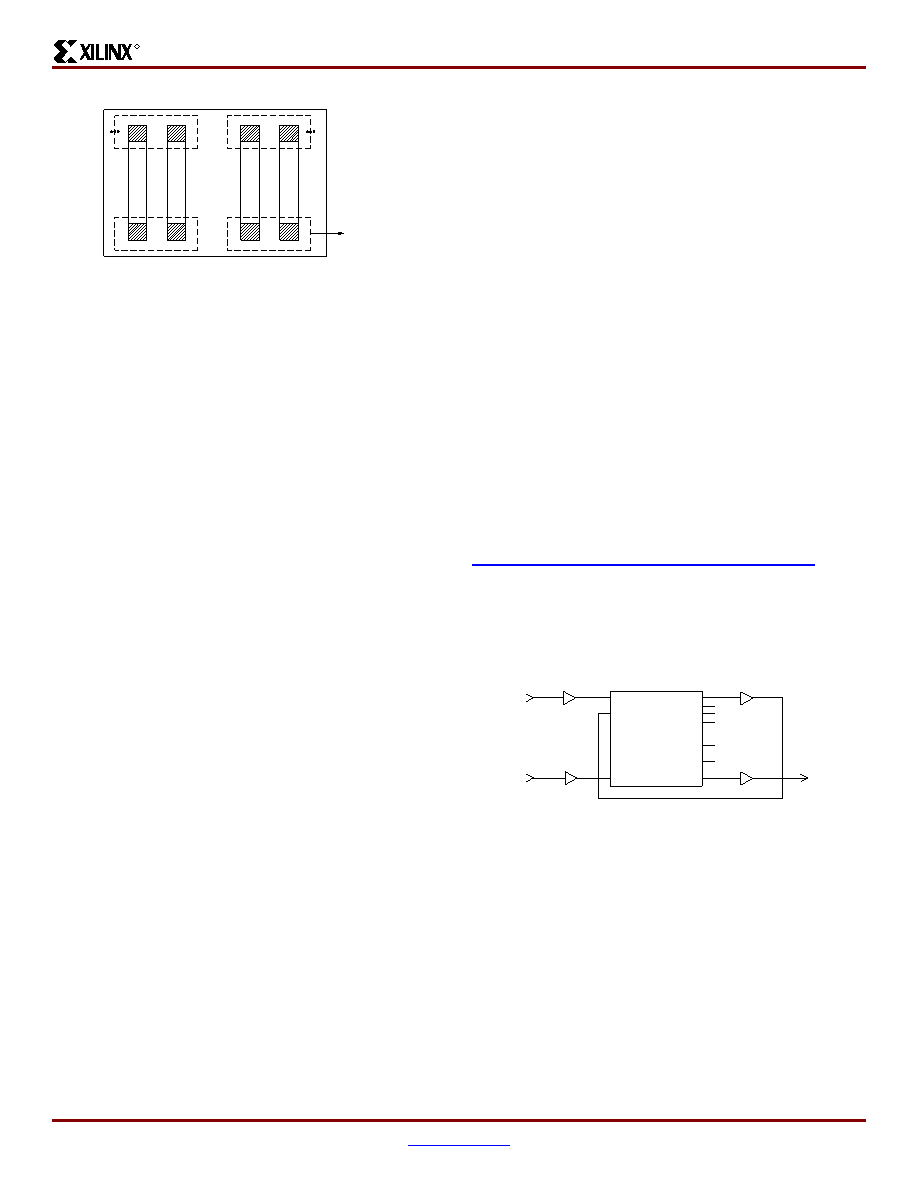
Figure 26: Virtex Series DLLs
x132_14_100799
B
R
A
M
DLL-3P
DLL-1P
DLL-3S
DLL-1S
DLL-2S
DLL-0S
DLL-2P
DLL-0P
Bottom Right
Half Edge
B
R
A
M
B
R
A
M
B
R
A
M
Figure 27: Standard DLL Implementation
CLK0
CLK90
CLK180
CLK270
CLK2X
CLKDV
LOCKED
CLKIN
CLKFB
RST
ds022_028_121099
CLKDLL
BUFG
IBUFG
IBUF
OBUF
相关PDF资料 |
PDF描述 |
|---|---|
| AMM36DRUH | CONN EDGECARD 72POS .156 DIP SLD |
| FMM28DSEN-S243 | CONN EDGECARD 56POS .156 EYELET |
| XC5VLX110-2FF1760C | IC FPGA VIRTEX-5 110K 1760FBGA |
| XC5VLX110-2FF1153C | IC FPGA VIRTEX-5 110K 1153FBGA |
| XC6VLX240T-1FFG1156I | IC FPGA VIRTEX 6 241K 1156FFGBGA |
相关代理商/技术参数 |
参数描述 |
|---|---|
| XCV812E-7BG560I | 制造商:XILINX 制造商全称:XILINX 功能描述:Virtex-E 1.8 V Extended Memory Field Programmable Gate Arrays |
| XCV812E-7BG676C | 制造商:XILINX 制造商全称:XILINX 功能描述:Virtex-E 1.8 V Extended Memory Field Programmable Gate Arrays |
| XCV812E-7BG676I | 制造商:XILINX 制造商全称:XILINX 功能描述:Virtex-E 1.8 V Extended Memory Field Programmable Gate Arrays |
| XCV812E-7BG900C | 制造商:XILINX 制造商全称:XILINX 功能描述:Virtex-E 1.8 V Extended Memory Field Programmable Gate Arrays |
| XCV812E-7BG900I | 制造商:XILINX 制造商全称:XILINX 功能描述:Virtex-E 1.8 V Extended Memory Field Programmable Gate Arrays |
发布紧急采购,3分钟左右您将得到回复。