参数资料
| 型号: | XCV812E-7BG560C |
| 厂商: | Xilinx Inc |
| 文件页数: | 63/118页 |
| 文件大小: | 0K |
| 描述: | IC FPGA 1.8V C-TEMP 560-MBGA |
| 产品变化通告: | FPGA Family Discontinuation 18/Apr/2011 |
| 标准包装: | 1 |
| 系列: | Virtex®-E EM |
| LAB/CLB数: | 4704 |
| 逻辑元件/单元数: | 21168 |
| RAM 位总计: | 1146880 |
| 输入/输出数: | 404 |
| 门数: | 254016 |
| 电源电压: | 1.71 V ~ 1.89 V |
| 安装类型: | 表面贴装 |
| 工作温度: | 0°C ~ 85°C |
| 封装/外壳: | 560-LBGA,金属 |
| 供应商设备封装: | 560-MBGA(42.5x42.5) |
第1页第2页第3页第4页第5页第6页第7页第8页第9页第10页第11页第12页第13页第14页第15页第16页第17页第18页第19页第20页第21页第22页第23页第24页第25页第26页第27页第28页第29页第30页第31页第32页第33页第34页第35页第36页第37页第38页第39页第40页第41页第42页第43页第44页第45页第46页第47页第48页第49页第50页第51页第52页第53页第54页第55页第56页第57页第58页第59页第60页第61页第62页当前第63页第64页第65页第66页第67页第68页第69页第70页第71页第72页第73页第74页第75页第76页第77页第78页第79页第80页第81页第82页第83页第84页第85页第86页第87页第88页第89页第90页第91页第92页第93页第94页第95页第96页第97页第98页第99页第100页第101页第102页第103页第104页第105页第106页第107页第108页第109页第110页第111页第112页第113页第114页第115页第116页第117页第118页
Virtex-E 1.8 V Extended Memory Field Programmable Gate Arrays
DS025-2 (v3.0) March 21, 2014
Module 2 of 4
45
R
— OBSOLETE — OBSOLETE — OBSOLETE — OBSOLETE —
LVDS
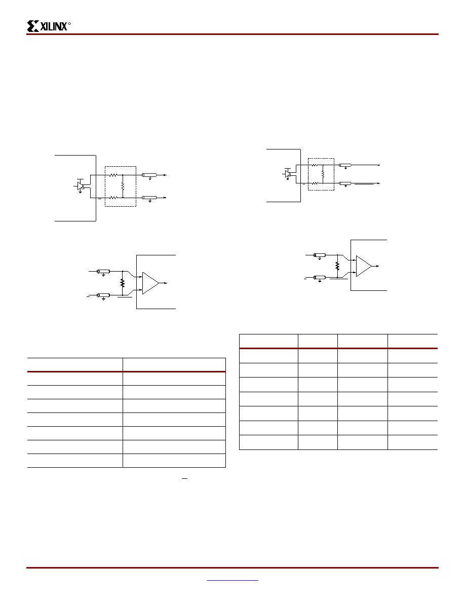
Depending on whether the device is transmitting an LVDS
signal or receiving an LVDS signal, there are two different
circuits used for LVDS termination. A sample circuit illustrat-
ing a valid termination technique for transmitting LVDS sig-
nals appears in Figure 54. A sample circuit illustrating a
valid termination for receiving LVDS signals appears in
information on the specific termination resistor packs shown
can be found on Table 40.
LVPECL
Depending on whether the device is transmitting or receiv-
ing an LVPECL signal, two different circuits are used for
LVPECL termination. A sample circuit illustrating a valid ter-
mination
technique
for
transmitting
LVPECL
signals
appears in Figure 56. A sample circuit illustrating a valid ter-
mination
for
receiving
LVPECL
signals
appears
in
Figure 57. Table 39 lists DC voltage specifications. Further
information on the specific termination resistor packs shown
can be found on Table 40.
Figure 54: Transmitting LVDS Signal Circuit
Figure 55: Receiving LVDS Signal Circuit
Table 38:
LVDS Voltage Specifications
Parameter
Min
Typ
Max
VCCO
2.375
2.5
2.625
VICM(2)
0.2
1.25
2.2
VOCM(1)
1.125
1.25
1.375
VIDIFF (1)
0.1
0.35
-
VODIFF (1)
0.25
0.35
0.45
VOH(1)
1.25
-
VOL(1)
-
1.25
Notes:
1.
Measured with a 100
Ω resistor across Q and Q.
2.
Measured with a differential input voltage =
+/ 350 mV.
x133_19_122799
Q
Z0 = 50Ω
Q
Virtex-E
FPGA
to LVDS Receiver
RDIV
140
R
S
165
R
S
165
2.5V
V
CCO = 2.5V
LVDS
Output
DATA
Transmit
1/4 of Bourns
Part Number
CAT16-LV4F12
x133_29_122799
Q
Z0 = 50Ω
LVDS_IN
Z0 = 50Ω
R
T
100
Ω
Q
DATA
Receive
from
LVDS
Driver
VIRTEX-E
FPGA
+
–
Figure 56: Transmitting LVPECL Signal Circuit
Figure 57: Receiving LVPECL Signal Circuit
Table 39:
LVPECL Voltage Specifications
Parameter
Min
Typ
Max
VCCO
3.0
3.3
3.6
VREF
--
-
VTT
--
-
VIH
1.49
-
2.72
VIL
0.86
-
2.125
VOH
1.8
-
VOL
-
1.57
Note: For more detailed information, see LVPECL DC
x133_20_122799
Q
Z0 = 50Ω LVPECL_OUT
LVPECL_OUT
Z0 = 50Ω
Q
Virtex-E
FPGA
to LVPECL Receiver
RDIV
187
R
S
100
R
S
100
3.3V
DATA
Transmit
1/4 of Bourns
Part Number
CAT16-PC4F12
x133_21_122799
Q
Z0 = 50Ω
LVPECL_IN
Z0 = 50Ω
R
T
100
Ω
Q
DATA
Receive
from
LVPECL
Driver
VIRTEX-E
FPGA
+
–
相关PDF资料 |
PDF描述 |
|---|---|
| AMM36DRUH | CONN EDGECARD 72POS .156 DIP SLD |
| FMM28DSEN-S243 | CONN EDGECARD 56POS .156 EYELET |
| XC5VLX110-2FF1760C | IC FPGA VIRTEX-5 110K 1760FBGA |
| XC5VLX110-2FF1153C | IC FPGA VIRTEX-5 110K 1153FBGA |
| XC6VLX240T-1FFG1156I | IC FPGA VIRTEX 6 241K 1156FFGBGA |
相关代理商/技术参数 |
参数描述 |
|---|---|
| XCV812E-7BG560I | 制造商:XILINX 制造商全称:XILINX 功能描述:Virtex-E 1.8 V Extended Memory Field Programmable Gate Arrays |
| XCV812E-7BG676C | 制造商:XILINX 制造商全称:XILINX 功能描述:Virtex-E 1.8 V Extended Memory Field Programmable Gate Arrays |
| XCV812E-7BG676I | 制造商:XILINX 制造商全称:XILINX 功能描述:Virtex-E 1.8 V Extended Memory Field Programmable Gate Arrays |
| XCV812E-7BG900C | 制造商:XILINX 制造商全称:XILINX 功能描述:Virtex-E 1.8 V Extended Memory Field Programmable Gate Arrays |
| XCV812E-7BG900I | 制造商:XILINX 制造商全称:XILINX 功能描述:Virtex-E 1.8 V Extended Memory Field Programmable Gate Arrays |
发布紧急采购,3分钟左右您将得到回复。