参数资料
| 型号: | XCV812E-7BG560C |
| 厂商: | Xilinx Inc |
| 文件页数: | 89/118页 |
| 文件大小: | 0K |
| 描述: | IC FPGA 1.8V C-TEMP 560-MBGA |
| 产品变化通告: | FPGA Family Discontinuation 18/Apr/2011 |
| 标准包装: | 1 |
| 系列: | Virtex®-E EM |
| LAB/CLB数: | 4704 |
| 逻辑元件/单元数: | 21168 |
| RAM 位总计: | 1146880 |
| 输入/输出数: | 404 |
| 门数: | 254016 |
| 电源电压: | 1.71 V ~ 1.89 V |
| 安装类型: | 表面贴装 |
| 工作温度: | 0°C ~ 85°C |
| 封装/外壳: | 560-LBGA,金属 |
| 供应商设备封装: | 560-MBGA(42.5x42.5) |
第1页第2页第3页第4页第5页第6页第7页第8页第9页第10页第11页第12页第13页第14页第15页第16页第17页第18页第19页第20页第21页第22页第23页第24页第25页第26页第27页第28页第29页第30页第31页第32页第33页第34页第35页第36页第37页第38页第39页第40页第41页第42页第43页第44页第45页第46页第47页第48页第49页第50页第51页第52页第53页第54页第55页第56页第57页第58页第59页第60页第61页第62页第63页第64页第65页第66页第67页第68页第69页第70页第71页第72页第73页第74页第75页第76页第77页第78页第79页第80页第81页第82页第83页第84页第85页第86页第87页第88页当前第89页第90页第91页第92页第93页第94页第95页第96页第97页第98页第99页第100页第101页第102页第103页第104页第105页第106页第107页第108页第109页第110页第111页第112页第113页第114页第115页第116页第117页第118页
Virtex-E 1.8 V Extended Memory Field Programmable Gate Arrays
Module 3 of 4
DS025-3 (v3.0) March 21, 2014
16
R
— OBSOLETE — OBSOLETE — OBSOLETE — OBSOLETE —
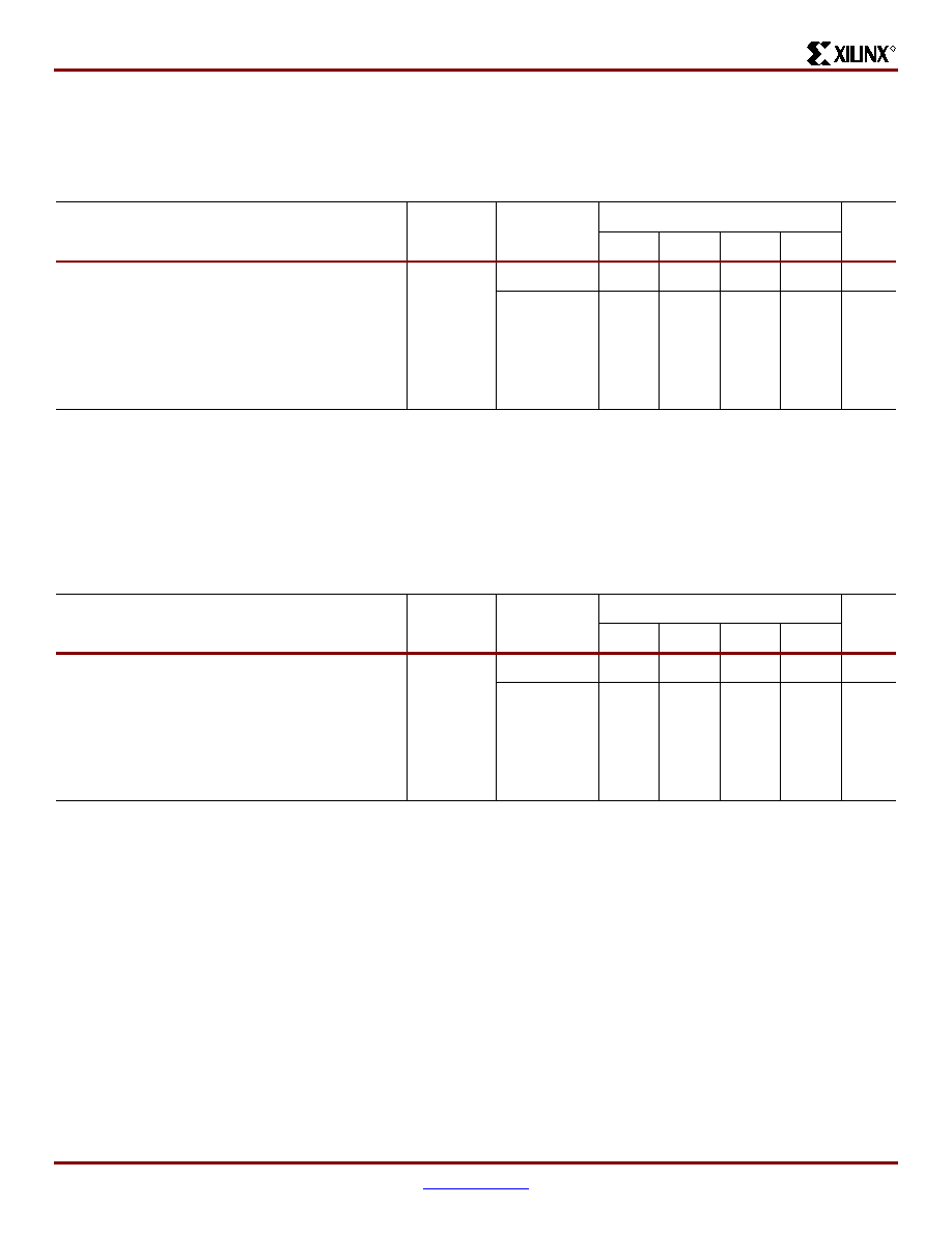
Virtex-E Pin-to-Pin Output Parameter Guidelines
All devices are 100% functionally tested. Listed below are representative values for typical pin locations and normal clock
loading. Values are expressed in nanoseconds unless otherwise noted.
Global Clock Input to Output Delay for LVTTL, 12 mA, Fast Slew Rate, with DLL
Global Clock Input to Output Delay for LVTTL, 12 mA, Fast Slew Rate, without DLL
Description(1)
Symbol
Device(3)
Speed Grade(2)
Units
Min
-8
-7
-6
LVTTL Global Clock Input to Output Delay using
Output Flip-flop, 12 mA, Fast Slew Rate, with
DLL.
For data output with different standards, adjust
the delays with the values shown in ‘‘IOB Output
TICKOFDLL
XCV405E
1.0
3.1
ns
XCV812E
1.0
3.1
ns
Notes:
1.
Listed above are representative values where one global clock input drives one vertical clock line in each accessible column, and
where all accessible IOB and CLB flip-flops are clocked by the global clock net.
2.
Output timing is measured at 50% VCC threshold with 35 pF external capacitive load. For other I/O standards and different loads, see
3.
DLL output jitter is already included in the timing calculation.
Description(1)
Symbol
Device
Speed Grade(2)
Units
Min
-8
-7
-6
LVTTL Global Clock Input to Output Delay using
Output Flip-flop, 12 mA, Fast Slew Rate, without
DLL.
For data output with different standards, adjust
the delays with the values shown in ‘‘IOB Output
TICKOF
XCV405E
1.6
4.5
4.7
4.9
ns
XCV812E
1.8
4.8
5.0
5.2
ns
Notes:
1.
Listed above are representative values where one global clock input drives one vertical clock line in each accessible column, and
where all accessible IOB and CLB flip-flops are clocked by the global clock net.
2.
Output timing is measured at 50% VCC threshold with 35 pF external capacitive load. For other I/O standards and different loads, see
相关PDF资料 |
PDF描述 |
|---|---|
| AMM36DRUH | CONN EDGECARD 72POS .156 DIP SLD |
| FMM28DSEN-S243 | CONN EDGECARD 56POS .156 EYELET |
| XC5VLX110-2FF1760C | IC FPGA VIRTEX-5 110K 1760FBGA |
| XC5VLX110-2FF1153C | IC FPGA VIRTEX-5 110K 1153FBGA |
| XC6VLX240T-1FFG1156I | IC FPGA VIRTEX 6 241K 1156FFGBGA |
相关代理商/技术参数 |
参数描述 |
|---|---|
| XCV812E-7BG560I | 制造商:XILINX 制造商全称:XILINX 功能描述:Virtex-E 1.8 V Extended Memory Field Programmable Gate Arrays |
| XCV812E-7BG676C | 制造商:XILINX 制造商全称:XILINX 功能描述:Virtex-E 1.8 V Extended Memory Field Programmable Gate Arrays |
| XCV812E-7BG676I | 制造商:XILINX 制造商全称:XILINX 功能描述:Virtex-E 1.8 V Extended Memory Field Programmable Gate Arrays |
| XCV812E-7BG900C | 制造商:XILINX 制造商全称:XILINX 功能描述:Virtex-E 1.8 V Extended Memory Field Programmable Gate Arrays |
| XCV812E-7BG900I | 制造商:XILINX 制造商全称:XILINX 功能描述:Virtex-E 1.8 V Extended Memory Field Programmable Gate Arrays |
发布紧急采购,3分钟左右您将得到回复。