参数资料
| 型号: | XIO2200AGGW |
| 厂商: | Texas Instruments |
| 文件页数: | 174/202页 |
| 文件大小: | 0K |
| 描述: | IC PCI-EXPRESS/BUS BRIDGE 176BGA |
| 产品培训模块: | PCI Express Basics |
| 标准包装: | 126 |
| 应用: | PCI Express 至 PCI 转换桥 |
| 接口: | PCI |
| 电源电压: | 1.35 V ~ 1.65 V,3 V ~ 3.6 V |
| 封装/外壳: | 176-LFBGA |
| 供应商设备封装: | 176-BGA MICROSTAR(15x15) |
| 包装: | 托盘 |
| 安装类型: | 表面贴装 |
| 产品目录页面: | 882 (CN2011-ZH PDF) |
| 配用: | XIO2200AEVM-ND - XIO2200AEVM |
| 其它名称: | 296-19617 |
第1页第2页第3页第4页第5页第6页第7页第8页第9页第10页第11页第12页第13页第14页第15页第16页第17页第18页第19页第20页第21页第22页第23页第24页第25页第26页第27页第28页第29页第30页第31页第32页第33页第34页第35页第36页第37页第38页第39页第40页第41页第42页第43页第44页第45页第46页第47页第48页第49页第50页第51页第52页第53页第54页第55页第56页第57页第58页第59页第60页第61页第62页第63页第64页第65页第66页第67页第68页第69页第70页第71页第72页第73页第74页第75页第76页第77页第78页第79页第80页第81页第82页第83页第84页第85页第86页第87页第88页第89页第90页第91页第92页第93页第94页第95页第96页第97页第98页第99页第100页第101页第102页第103页第104页第105页第106页第107页第108页第109页第110页第111页第112页第113页第114页第115页第116页第117页第118页第119页第120页第121页第122页第123页第124页第125页第126页第127页第128页第129页第130页第131页第132页第133页第134页第135页第136页第137页第138页第139页第140页第141页第142页第143页第144页第145页第146页第147页第148页第149页第150页第151页第152页第153页第154页第155页第156页第157页第158页第159页第160页第161页第162页第163页第164页第165页第166页第167页第168页第169页第170页第171页第172页第173页当前第174页第175页第176页第177页第178页第179页第180页第181页第182页第183页第184页第185页第186页第187页第188页第189页第190页第191页第192页第193页第194页第195页第196页第197页第198页第199页第200页第201页第202页
Classic PCI Configuration Space
60
March 5 2007 June 2011
SCPS154C
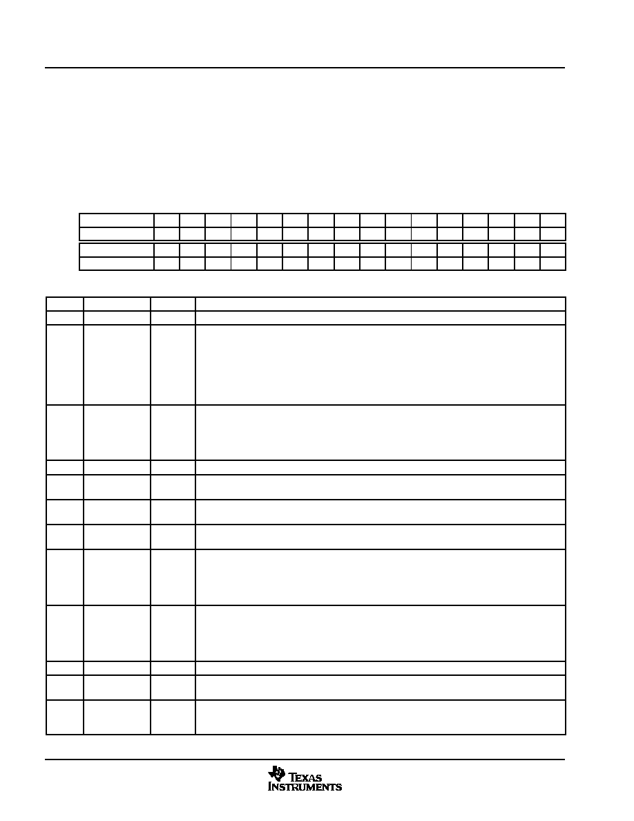
4.49 Device Capabilities Register
The device capabilities register indicates the device specific capabilities of the bridge. See Table 425 for a
complete description of the register contents.
PCI register offset:
94h
Register type:
Read-only
Default value:
0000 0D82
BIT NUMBER
31
30
29
28
27
26
25
24
23
22
21
20
19
18
17
16
RESET STATE
0
BIT NUMBER
15
14
13
12
11
10
9
8
7
6
5
4
3
2
1
0
RESET STATE
0
1
0
1
0
1
0
Table 425. Device Capabilities Register Description
BIT
FIELD NAME
ACCESS
DESCRIPTION
31:28
RSVD
R
Reserved. Returns 0h when read.
27:26
CSPLS
RU
Captured slot power limit scale. The value in this field is programmed by the host by issuing a
Set_Slot_Power_Limit message. When a Set_Slot_Power_Limit message is received, bits 9:8 are
written to this field. The value in this field specifies the scale used for the slot power limit.
00 = 1.0x
01 = 0.1x
10 = 0.01x
11 = 0.001x
25:18
CSPLV
RU
Captured slot power limit value. The value in this field is programmed by the host by issuing a
Set_Slot_Power_Limit message. When a Set_Slot_Power_Limit message is received, bits 7:0 are
written to this field. The value in this field in combination with the slot power limit scale value
(bits 27:26) specifies the upper limit of power supplied to the slot. The power limit is calculated by
multiplying the value in this field by the value in the slot power limit scale field.
17:15
RSVD
R
Reserved. Return 000b when read.
14
PIP
R
Power indicator present. This bit is hardwired to 0b indicating that a power indicator is not
implemented.
13
AIP
R
Attention indicator present. This bit is hardwired to 0b indicating that an attention indicator is not
implemented.
12
ABP
R
Attention button present. This bit is hardwired to 0b indicating that an attention button is not
implemented.
11:9
EP_L1_LAT
RU
Endpoint L1 acceptable latency. This field indicates the maximum acceptable latency for a
transition from L1 to L0 state. This field can be programmed by writing to the L1_LATENCY field
(bits 15:13) in the general control register (offset D4h, see Section 4.65). The default value for this
field is 110b which indicates a range from 32 μs to 64 μs. This field cannot be programmed to be
less than the latency for the PHY to exit the L1 state.
8:6
EP_L0S_LAT
RU
Endpoint L0s acceptable latency. This field indicates the maximum acceptable latency for a
transition from L0s to L0 state. This field can be programmed by writing to the L0s_LATENCY field
(bits 18:16) in the general control register (offset D4h, see Section 4.65). The default value for this
field is 110b which indicates a range from 2 μs to 4 μs. This field cannot be programmed to be less
than the latency for the PHY to exit the L0s state.
5
ETFS
R
Extended tag field supported. This field indicates the size of the tag field not supported.
4:3
PFS
R
Phantom functions supported. This field is read-only 00b indicating that function numbers are not
used for phantom functions.
2:0
MPSS
R
Maximum payload size supported. This field indicates the maximum payload size that the device
can support for TLPs. This field is encoded as 010b indicating the maximum payload size for a TLP
is 512 bytes.
Not Recommended for New Designs
相关PDF资料 |
PDF描述 |
|---|---|
| XIO2200AZGW | IC PCI-EXPRESS/BUS BRIDGE 176BGA |
| XPC823ZT81B2T | IC MPU POWERQUICC 81MHZ 256-PBGA |
| XPC8240RZU250E | MCU HOST PROCESSOR 352-TBGA |
| XQ6SLX150T-3CSG484I | IC FPGA SPARTAN-6Q 484-CSBGA |
| XR16C2550IJ-F | IC UART FIFO 16B DUAL 44PLCC |
相关代理商/技术参数 |
参数描述 |
|---|---|
| XIO2200AZGW | 功能描述:外围驱动器与原件 - PCI PCI Exp-PCI Bus Trans Bridge RoHS:否 制造商:PLX Technology 工作电源电压: 最大工作温度: 安装风格:SMD/SMT 封装 / 箱体:FCBGA-1156 封装:Tray |
| XIO2200AZGW | 制造商:Texas Instruments 功能描述:PCI Express to PCI Bus Converter IC |
| XIO2200AZHH | 功能描述:外围驱动器与原件 - PCI PCI Exp-PCI Bus Trans Bridge RoHS:否 制造商:PLX Technology 工作电源电压: 最大工作温度: 安装风格:SMD/SMT 封装 / 箱体:FCBGA-1156 封装:Tray |
| XIO2200GGW | 功能描述:IC PCI-EXPRESS/BUS BRIDGE 176BGA RoHS:是 类别:集成电路 (IC) >> 接口 - 专用 系列:- 标准包装:3,000 系列:- 应用:PDA,便携式音频/视频,智能电话 接口:I²C,2 线串口 电源电压:1.65 V ~ 3.6 V 封装/外壳:24-WQFN 裸露焊盘 供应商设备封装:24-QFN 裸露焊盘(4x4) 包装:带卷 (TR) 安装类型:表面贴装 产品目录页面:1015 (CN2011-ZH PDF) 其它名称:296-25223-2 |
| XIO2200ZGW | 功能描述:IC PCI-EXPRESS/BUS BRIDGE 176BGA RoHS:是 类别:集成电路 (IC) >> 接口 - 专用 系列:- 标准包装:3,000 系列:- 应用:PDA,便携式音频/视频,智能电话 接口:I²C,2 线串口 电源电压:1.65 V ~ 3.6 V 封装/外壳:24-WQFN 裸露焊盘 供应商设备封装:24-QFN 裸露焊盘(4x4) 包装:带卷 (TR) 安装类型:表面贴装 产品目录页面:1015 (CN2011-ZH PDF) 其它名称:296-25223-2 |
发布紧急采购,3分钟左右您将得到回复。