- 您现在的位置:买卖IC网 > PDF目录370033 > 256MBDDRSDRAM (SAMSUNG SEMICONDUCTOR CO. LTD.) DDR SDRAM Specification Version 0.3 PDF资料下载
参数资料
| 型号: | 256MBDDRSDRAM |
| 厂商: | SAMSUNG SEMICONDUCTOR CO. LTD. |
| 英文描述: | DDR SDRAM Specification Version 0.3 |
| 中文描述: | DDR SDRAM的规格版本0.3 |
| 文件页数: | 25/51页 |
| 文件大小: | 658K |
| 代理商: | 256MBDDRSDRAM |
第1页第2页第3页第4页第5页第6页第7页第8页第9页第10页第11页第12页第13页第14页第15页第16页第17页第18页第19页第20页第21页第22页第23页第24页当前第25页第26页第27页第28页第29页第30页第31页第32页第33页第34页第35页第36页第37页第38页第39页第40页第41页第42页第43页第44页第45页第46页第47页第48页第49页第50页第51页
- 25 -
REV. 0.3 November 2. 2000
256Mb DDR SDRAM
Preliminary
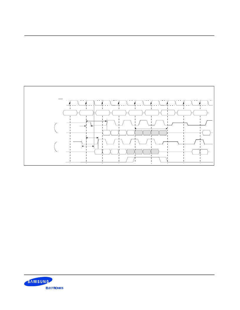
3.3.8 Write Interrupted by a Precharge & DM
A burst write operation can be interrupted before completion of the burst by a precharge of the same bank.
Random column access is allowed. A write recovery time(tWR) is required from the last data to precharge
command. When precharge command is asserted, any residual data from the burst write cycle must be
masked by DM.
Command
< Burst Length=8 >
NOP
WRITE A
NOP
NOP
Precharge
NOP
NOP
NOP
WRITEB
DQS
DQ
′
s
Dina
0
Dina
1
Dina
2
Dina
3
Dina
4
Dina
5
Dinb
0
Dina
6
Dina
7
t
WR
DQS
DQ
′
s
t
DQSSmin
Dina
7
Dina
0
Dina
1
Dina
2
Dina
3
Dina
4
Dina
5
Dina
6
DM
Dinb
0
Dinb
1
t
DQSSmax
2
0
1
5
3
4
8
6
7
CK
CK
Precharge timing for Write operations in DRAMs requires enough time to allow “write recovery” which is the
time required by a DRAM core to properly store a full “0” or “1” level before a Precharge operation. For DDR
SDRAM, a timing parameter, tWR, is used to indicate the required amount of time between the last valid write
operation and a Precharge command to the same bank.
The precharge timing for writes is a complex definition since the write data is sampled by the data strobe and
the address is sampled by the input clock. Inside the SDRAM, the data path is eventually synchronized with
the address path by switching clock domains from the data strobe clock domain to the input clock domain.
This makes the definition of when a precharge operation can be initiated after a write very complex since the
write recovery parameter must reference only the clock domain that is used to time the internal write operation,
i.e., the input clock domain.
tWR starts on the rising clock edge after the last possible DQS edge that strobed in the last valid data and
ends on the rising clock edge that strobes in the precharge command.
1. For the earliest possible Precharge command following a Write burst without interrupting the burst, the
minimum time for write recovery is defined by tWR.
2. When a precharge command interrupts a Write burst operation, the data mask pin, DM, is used to mask
input data during the time between the last valid write data and the rising clock edge on which the
Precharge command is given. During this time, the DQS input is still required to strobe in the state of DM.
The minimum time for write recovery is defined by tWR.
Figure 16. Write interrupted by a precharge and DM timing
t
WPRES*5
t
WPRES*5
相关PDF资料 |
PDF描述 |
|---|---|
| 25AV5-GA | FOR TV HORIZONTAL-DEFLECTION AMPLIFIER APPLICATIONS |
| 25CV100BE | Surface Mount Type Miniature, Super low profile 3.9mm height |
| 25CV10BE | Surface Mount Type Miniature, Super low profile 3.9mm height |
| 25CV68BE | Surface Mount Type Miniature, Super low profile 3.9mm height |
| 25CV22BE | Surface Mount Type Miniature, Super low profile 3.9mm height |
相关代理商/技术参数 |
参数描述 |
|---|---|
| 256MB-FD | 制造商:PNY Technologies 功能描述:256MB USB, FOR IBM - Bulk |
| 256MB-FLASH | 制造商:STMicroelectronics 功能描述: |
| 256ME-250K | 制造商:ILLINOISCAPACITOR 制造商全称:Illinois Capacitor, Inc. 功能描述:Metallized Polyester Motor Run/AC Film Capacitors In Boxes |
| 256ME-350K | 制造商:ILLINOISCAPACITOR 制造商全称:Illinois Capacitor, Inc. 功能描述:Metallized Polyester Motor Run/AC Film Capacitors In Boxes |
| 256ME-400K | 制造商:ILLINOISCAPACITOR 制造商全称:Illinois Capacitor, Inc. 功能描述:Metallized Polyester Motor Run/AC Film Capacitors In Boxes |
发布紧急采购,3分钟左右您将得到回复。