- 您现在的位置:买卖IC网 > PDF目录373890 > AD6623PCB (Analog Devices, Inc.) 4-Channel, 104 MSPS Digital Transmit Signal Processor TSP PDF资料下载
参数资料
| 型号: | AD6623PCB |
| 厂商: | Analog Devices, Inc. |
| 英文描述: | 4-Channel, 104 MSPS Digital Transmit Signal Processor TSP |
| 中文描述: | 4通道,104 MSPS的数字传输信号处理器判刑 |
| 文件页数: | 19/40页 |
| 文件大小: | 381K |
| 代理商: | AD6623PCB |
第1页第2页第3页第4页第5页第6页第7页第8页第9页第10页第11页第12页第13页第14页第15页第16页第17页第18页当前第19页第20页第21页第22页第23页第24页第25页第26页第27页第28页第29页第30页第31页第32页第33页第34页第35页第36页第37页第38页第39页第40页
REV. 0
AD6623
–19–
Table V. RCF Control Registers
Channel
Address
Bit
Width
Description
0x0A
0x0B
0x0C
16
8
10
15
–
8: N
RCF
–
1 B; 7
–
0: N
RCF
–
1 A
7
–
0: O
RCF
9: Ch. A Compact FIR Input Word Length
0: 16 bits
–
8 I followed by 8 Q
1: 24 bits
–
12 I followed by 12 Q
8: Ch. A RCF PRBS Enable
7: Ch A RCF PRBS Length
0: 15
1: 8,388,607
6
–
4: Ch. A RCF Mode Select
000 = FIR
001 = p/4-DQPSK Modulator
010 = GMSK Look-Up Table
011 = MSK Look-Up Table
100 = FIR compact mode
101 = 8-PSK
110 = 3p/8-8PSK Modulator
111 = QPSK Look-Up Table
3
–
0: Ch. A RCF Taps per Phase
7
–
6: RCF Coarse Scale (g):
00 = 0 dB
01 =
–
6 dB
10 =
–
12 dB
11 =
–
18 dB
5: Ch. A Allpass Ph. Eq. Enable
4
–
0: Serial Clock Divider (1, ..., 32)
15
–
2: Ch. A Unsigned Scale Factor
1
–
0: Reserved
17
–
16: Ch. A Time Slot Sync Select
00: Sync0 (See 0x001 Time Slot)
01: Sync1
10: Sync2
11: Sync3
15
–
0: Ch. A RCF Scale Hold-Off Counter
1) Ramp Down (if Ramp is enabled)
2) Update Scale and Mode
3) Ramp Up (if Ramp is enabled)
15
–
0: Ch. A RCF Phase EQ Coef1
15
–
0: Ch. A RCF Phase EQ Coef2
15
–
0: Ch. A RCF MPSK Magnitude 0
15
–
0: Ch. A RCF MPSK Magnitude 1
15
–
0: Ch. A RCF MPSK Magnitude 2
15
–
0: Ch. A RCF MPSK Magnitude 3
7: Reserved
6: Ch. A Serial Data Frame Select
0: Serial Data Frame Request
1: Serial Data Frame End
0x0D
8
0x0E
16
0x0F
18
0x110
0x111
0x112
0x113
0x114
0x115
0x116
16
16
16
16
16
16
8
Channel
Address
Bit
Width Description
5: Ch. A External SDFI Select
0: Internal SDFI
1: External SDFI
4: Ch. A SCLK Slave Select
0: Master
1: Slave
3: Ch. A Serial Fine Scale Enable
2: Ch. A Serial Time Slot Sync Enable
(ignored in FIR mode)
1: Ch. A Ramp Interpolation Enable
0: Ch. A Ramp Enable
5
–
0: Ch. A Mode 0 Ramp Length, R0
–
1
5
–
0: Ch. A Mode 1 Ramp Length, R1
–
1
4
–
0: Ch. A Ramp Rest Time, Q
Reserved
15
–
0: Ch. A Data Memory
15
–
14: Reserved
13
–
0: Ch. A Power Ramp Memory
15
–
0: Ch. A Coefficient Memory
This address is mirrored at 0x900
–
0x97F
and contiguously extended at
0x980
–
0x9FF
0x117
0x118
0x119
0x11A
–
0x11F
0x120
–
0x13F 16
0x140
–
0x17F 16
6
6
5
0x180
–
0x1FF 16
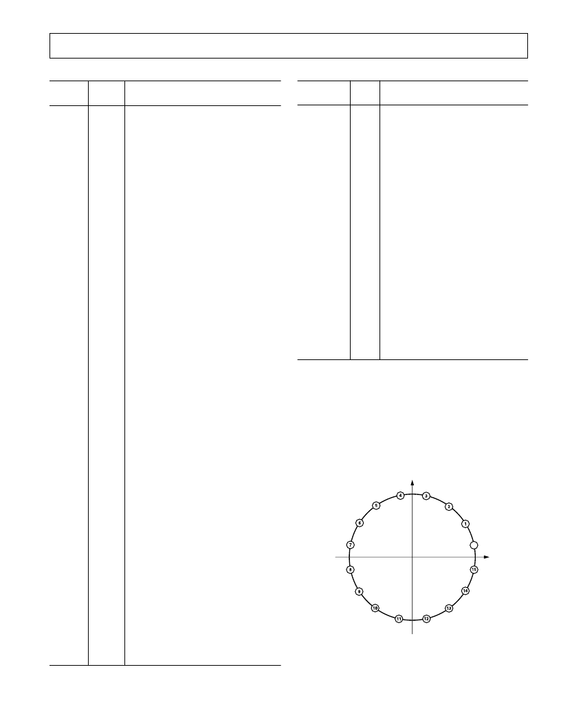
PSK MODULATOR
The PSK Modulator is an AD6623 extension feature that is
only available when the control register bit 0x000:7 is high.
The PSK Modulator creates 32-bit complex inputs to the
Interpolating FIR Filter from two or three data bits captured
by the serial port. The FIR Filter operates exactly as if the 32-
bit word came directly from the serial port. There are three
PSK modulation options to choose from: /4-DQPSK, 8-PSK,
and 3 /8-8-PSK. Every symbol of any of these modulations
can be represented by one of the 16 phases shown in Figure 21.
0
Figure 21. 16-Phase Modulations
相关PDF资料 |
PDF描述 |
|---|---|
| AD6624AS | Four-Channel, 80 MSPS Digital Receive Signal Processor (RSP) |
| AD6624A | Four-Channel, 100 MSPS Digital Receive Signal Processor (RSP) |
| AD6624AABC | Four-Channel, 100 MSPS Digital Receive Signal Processor (RSP) |
| AD6630AR-REEL | Differential, Low Noise IF Gain Block with Output Clamping |
| AD6630AR | Differential, Low Noise IF Gain Block with Output Clamping |
相关代理商/技术参数 |
参数描述 |
|---|---|
| AD6623S/PCB | 制造商:Analog Devices 功能描述:4-CH, 104 MSPS DGTL TRANSMIT SGNL PROCESSOR (TSP) 28SOIC - Bulk |
| AD6624 | 制造商:AD 制造商全称:Analog Devices 功能描述:Four-Channel, 80 MSPS Digital Receive Signal Processor (RSP) |
| AD6624A | 制造商:AD 制造商全称:Analog Devices 功能描述:Four-Channel, 100 MSPS Digital Receive Signal Processor (RSP) |
| AD6624AABC | 制造商:Advanced Micro Devices 功能描述: |
| AD6624AABCZ | 功能描述:DIGITAL SIGNAL PROC 196 CSP-BGA RoHS:是 类别:集成电路 (IC) >> 专用 IC 系列:* 产品培训模块:Lead (SnPb) Finish for COTS Obsolescence Mitigation Program 标准包装:1 系列:- 类型:调帧器 应用:数据传输 安装类型:表面贴装 封装/外壳:400-BBGA 供应商设备封装:400-PBGA(27x27) 包装:散装 |
发布紧急采购,3分钟左右您将得到回复。