参数资料
| 型号: | AD7294BCPZRL |
| 厂商: | Analog Devices Inc |
| 文件页数: | 14/49页 |
| 文件大小: | 0K |
| 描述: | IC ADC 12BIT I2C/SRL 1M 56LFCSP |
| 标准包装: | 2,500 |
| 类型: | ADC,DAC |
| 分辨率(位): | 12 b |
| 采样率(每秒): | 22.22k |
| 数据接口: | I²C,串行 |
| 电压电源: | 模拟和数字 |
| 电源电压: | 4.4 V ~ 5.5 V |
| 工作温度: | -40°C ~ 105°C |
| 安装类型: | 表面贴装 |
| 封装/外壳: | 56-VFQFN 裸露焊盘,CSP |
| 供应商设备封装: | 56-LFCSP-VQ(8x8) |
| 包装: | 带卷 (TR) |
第1页第2页第3页第4页第5页第6页第7页第8页第9页第10页第11页第12页第13页当前第14页第15页第16页第17页第18页第19页第20页第21页第22页第23页第24页第25页第26页第27页第28页第29页第30页第31页第32页第33页第34页第35页第36页第37页第38页第39页第40页第41页第42页第43页第44页第45页第46页第47页第48页第49页
AD7294
Data Sheet
Rev. H | Page 20 of 48
THEORY OF OPERATION
ADC OVERVIEW
The AD7294 provides the user with a 9-channel multiplexer, an
on-chip track-and-hold, and a successive approximation ADC
based around a capacitive DAC. The analog input range for the
part can be selected as a 0 V to VREF input or a 2 × VREF input,
configured with either single-ended or differential analog inputs.
The AD7294 has an on-chip 2.5 V reference that can be disabled
when an external reference is preferred. If the internal ADC
reference is to be used elsewhere in a system, the output must
first be buffered.
The various monitored and uncommitted input signals are multi-
plexed into the ADC. The AD7294 has four uncommitted
analog input channels, VIN0 to VIN3. These four channels allow
single-ended, differential, and pseudo differential mode
measurements of various system signals.
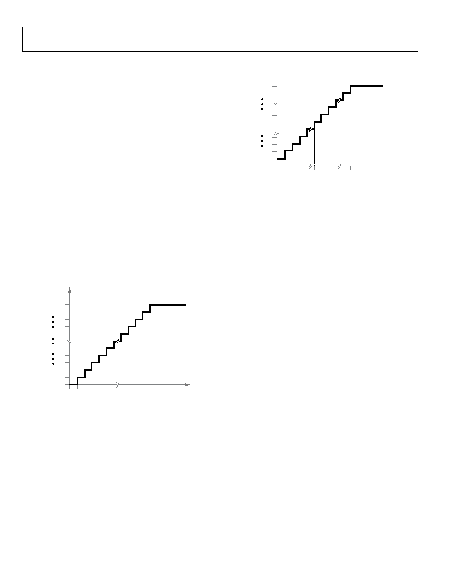
ADC TRANSFER FUNCTIONS
The designed code transitions occur at successive integer LSB
values (1 LSB, 2 LSB, and so on). In single-ended mode, the
LSB size is VREF/4096 when the 0 V to VREF range is used and
2 × VREF/4096 when the 0 V to 2 × VREF range is used. The ideal
transfer characteristic for the ADC when outputting straight
binary coding is shown in Figure 35.
000...000
111...111
1LSB = VREF/4096
1LSB
VREF – 1LSB
ANALOG INPUT
ADC
CO
DE
0V
000...001
000...010
111...110
111...000
011...111
NOTE
1. VREF IS EITHER VREF OR 2 × VREF.
05747-
016
Figure 35. Single-Ended Transfer Characteristic
In differential mode, the LSB size is 2 × VREF/4096 when the 0 V
to VREF range is used, and 4 × VREF/4096 when the 0 V to 2 × VREF
range is used. The ideal transfer characteristic for the ADC when
outputting twos complement coding is shown in Figure 36 (with
the 2 × VREF range).
100...000
011...111
1LSB = 2 × VREF/4096
+VREF – 1LSB
–VREF + 1LSB VREF – 1LSB
ANALOG INPUT
ADC
CO
DE
100...001
100...010
011...110
000...001
000...000
111...111
05747-
017
Figure 36. Differential Transfer Characteristic with VREF ± VREF Input Range
For VIN0 to VIN3 in single-ended mode, the output code is
straight binary, where
VIN = 0 V, DOUT = x000, VIN = VREF 1 LSB, and DOUT = xFFF
In differential mode, the code is twos complement, where
VIN+ VIN = 0 V, and DOUT = x00
VIN+ VIN = VREF 1 LSB, and DOUT = x7FF
VIN+ VIN = VREF, and DOUT = x800
Channel 5 and Channel 6 (current sensor inputs) are twos
complement, where
VIN+ VIN = 0 mV, and DOUT = x000
VIN+ VIN = VREF/12.5 1 LSB, DOUT = x7FF
VIN+ VIN = VREF/12.5, DOUT = x800
Channel 7 to Channel 9 (temperature sensor inputs) are twos
complement with the LSB equal to 0.25°C, where
TIN = 0°C, and DOUT = x000
TIN = +255.75°C, and DOUT = x7FF
TIN = 256°C, and DOUT = x800
ANALOG INPUTS
The AD7294 has a total of four analog inputs. Depending on
the configuration register setup, they can be configured as two
single-ended inputs, two pseudo differential channels, or two
fully differential channels. See the Register Setting section for
further details.
Single-Ended Mode
The AD7294 can have four single-ended analog input channels.
In applications where the signal source has high impedance, it is
recommended to buffer the analog input before applying it to the
ADC. The analog input range can be programmed to be either
0 V to VREF or 0 V to 2 × VREF. In 2 × VREF mode, the input is
effectively divided by 2 before the conversion takes place. Note
that the voltage with respect to GND on the ADC analog input
pins cannot exceed AVDD.
If the analog input signal to be sampled is bipolar, the internal
reference of the ADC can be used to externally bias up this
相关PDF资料 |
PDF描述 |
|---|---|
| AD7306AN | IC TXRX RS-232 RS-422 24-DIP |
| AD7339BSZ-REEL | IC ADC/QUAD DAC 5V W/REF 52-MQFP |
| AD7376ARUZ100 | IC POT DIGITAL 128POS 14-TSSOP |
| AD7391SRZ | IC DAC 10BIT SERIAL 3V 8SOIC |
| AD7392AR | IC DAC 12BIT PARALLEL 3V 20-SOIC |
相关代理商/技术参数 |
参数描述 |
|---|---|
| AD7294BSUZ | 功能描述:模数转换器 - ADC 12B Monitor & Cntrl System w/ Temp Sensr RoHS:否 制造商:Analog Devices 通道数量: 结构: 转换速率: 分辨率: 输入类型: 信噪比: 接口类型: 工作电源电压: 最大工作温度: 安装风格: 封装 / 箱体: |
| AD7294BSUZRL | 制造商:Analog Devices 功能描述:Temp Sensor Digital Serial (2-Wire, I2C) 64-Pin TQFP 制造商:Analog Devices 功能描述:TEMP SENSOR DGTL SERL (2-WIRE, I2C) 64TQFP - Tape and Reel 制造商:Analog Devices 功能描述:IC ADC 12BIT W/DAC/TEMP 64TQFP 制造商:Analog Devices Inc. 功能描述:Analog to Digital Converters - ADC 12-Bit Multi-Channel ADC DAC wt Temp IC 制造商:Analog Devices 功能描述:CONVERTER - ADC |
| AD7298 | 制造商:AD 制造商全称:Analog Devices 功能描述:8-Channel, 1MSPS, 12-Bit SAR ADC with Temperature Sensor |
| AD7298-1BCPZ | 功能描述:IC ADC 10BIT SPI/SRL 8CH 20LFCSP RoHS:是 类别:集成电路 (IC) >> 数据采集 - 模数转换器 系列:- 其它有关文件:TSA1204 View All Specifications 标准包装:1 系列:- 位数:12 采样率(每秒):20M 数据接口:并联 转换器数目:2 功率耗散(最大):155mW 电压电源:模拟和数字 工作温度:-40°C ~ 85°C 安装类型:表面贴装 封装/外壳:48-TQFP 供应商设备封装:48-TQFP(7x7) 包装:Digi-Reel® 输入数目和类型:4 个单端,单极;2 个差分,单极 产品目录页面:1156 (CN2011-ZH PDF) 其它名称:497-5435-6 |
| AD7298-1BCPZ-RL | 功能描述:IC ADC 10BIT SPI/SRL 8CH 20LFCSP RoHS:是 类别:集成电路 (IC) >> 数据采集 - 模数转换器 系列:- 标准包装:2,500 系列:- 位数:16 采样率(每秒):15 数据接口:MICROWIRE?,串行,SPI? 转换器数目:1 功率耗散(最大):480µW 电压电源:单电源 工作温度:-40°C ~ 85°C 安装类型:表面贴装 封装/外壳:38-WFQFN 裸露焊盘 供应商设备封装:38-QFN(5x7) 包装:带卷 (TR) 输入数目和类型:16 个单端,双极;8 个差分,双极 配用:DC1011A-C-ND - BOARD DELTA SIGMA ADC LTC2494 |
发布紧急采购,3分钟左右您将得到回复。