参数资料
| 型号: | AD7294BCPZRL |
| 厂商: | Analog Devices Inc |
| 文件页数: | 35/49页 |
| 文件大小: | 0K |
| 描述: | IC ADC 12BIT I2C/SRL 1M 56LFCSP |
| 标准包装: | 2,500 |
| 类型: | ADC,DAC |
| 分辨率(位): | 12 b |
| 采样率(每秒): | 22.22k |
| 数据接口: | I²C,串行 |
| 电压电源: | 模拟和数字 |
| 电源电压: | 4.4 V ~ 5.5 V |
| 工作温度: | -40°C ~ 105°C |
| 安装类型: | 表面贴装 |
| 封装/外壳: | 56-VFQFN 裸露焊盘,CSP |
| 供应商设备封装: | 56-LFCSP-VQ(8x8) |
| 包装: | 带卷 (TR) |
第1页第2页第3页第4页第5页第6页第7页第8页第9页第10页第11页第12页第13页第14页第15页第16页第17页第18页第19页第20页第21页第22页第23页第24页第25页第26页第27页第28页第29页第30页第31页第32页第33页第34页当前第35页第36页第37页第38页第39页第40页第41页第42页第43页第44页第45页第46页第47页第48页第49页
Data Sheet
AD7294
Rev. H | Page 39 of 48
MODES OF OPERATION
There are two different methods of initiating a conversion on
the AD7294: command mode and autocycle mode.
COMMAND MODE
In command mode, the AD7294 ADC converts on-demand on
either a single channel or a sequence of channels. To enter this
mode, the required combination of channels is written into the
command register (0x00). The first conversion takes place at the
end of this write operation, in time for the result to be read out
in the next read operation. While this result is being read out,
the next conversion in the sequence takes place, and so on.
To exit the command mode, the master should not acknowledge
the final byte of data. This stops the AD7294 transmitting,
allowing the master to assert a stop condition on the bus. It is
therefore important that, after writing to the command register,
a repeated start (Sr) signal be used rather than a stop (P) followed
by a start (S) when switching to read mode; otherwise, the
command mode exits after the first conversion.
After writing to the command register, the register pointer is
returned to its previous value. If a new pointer value is required
(typically the ADC Result Register 0x01), it can be written
immediately following the command byte. This extra write
operation does not affect the conversion sequence because the
second conversion triggers only at the start of the first read
operation.
The maximum throughput that can be achieved using this
mode with a 400 kHz I2C clock is (400 kHz/18) = 22.2 kSPS.
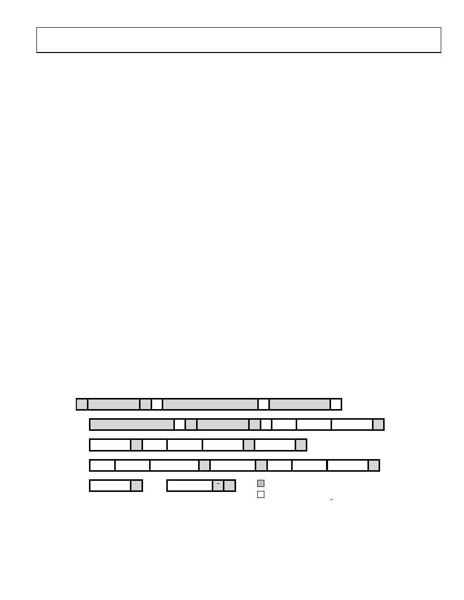
Figure 56 shows the command mode converting on a sequence
of channels including VIN0, VIN1, and ISENSE1.
1. The master device asserts a start condition on SDA.
2. The master sends the 7-bit slave address followed by the
write bit (low).
3. The addressed slave device (AD7294) asserts an
acknowledge on SDA.
4. The master sends the Command Register Address 0x00.
The slave asserts an acknowledge on SDA.
5. The master sends the Data Byte 0x13 which selects the
VIN0, VIN1, and ISENSE1 channels.
6. The slave asserts an acknowledge on SDA.
7. The master sends the result register address (0x01). The
slave asserts an acknowledge on SDA.
8. The master sends the 7-bit slave address followed by the
write bit (high).
9. The slave (AD7294) asserts an acknowledge on SDA.
10. The master receives a data byte, which contains the
alert_flag bit, the channel ID bits, and the four MSBs of the
converted result for Channel VIN0. The master then asserts
an acknowledge on SDA.
11. The master receives the second data byte, which contains
the eight LSBs of the converted result for Channel VIN0.
The master then asserts on acknowledge on SDA.
12. Point 10 and Point 11 repeat for Channel VIN1 and
Channel ISENSE1.
13. Once the master has received the results from all the
selected channels, the slave again converts and outputs
the result for the first channel in the selected sequence.
Point 10 to Point 12 are repeated.
14. The master asserts a no acknowledge on SDA and a stop
condition on SDA to end the conversion and exit
command mode.
The AD7294 automatically exits command mode if no read
occurs in a 5 ms period. To change the conversion sequence,
rewrite a new sequence to the command mode.
05747-
056
S
A
P
...
0
A
COMMAND = 0x13
A
VIN0<11:8>
A
POINT TO RESULT REG (0x01)
SR
1
A
*
A
CH ID (000)
ALERT?
...
A
CH ID (001)
ALERT?
A
...
A
ISENSE1<11:8>
*
A
...
A
VIN0<7:0>
...
........
A
* = POSITION OF A CONVERSION START
SLAVE ADDRESS
POINT TO COMMAND REG (0x00)
VIN1<7:0>
VIN0<7:0>
VIN1<11:8>
VIN0<11:8>
SLAVE ADDRESS
ISENSE1<7:0>
ALERT?
CH ID (100)
ALERT?
CH ID (000)
FROM MASTER TO SLAVE
FROM SLAVE TO MASTER
S = START CONDITION
SR = REPEATED START
P = STOP CONDITION
A = ACKNOWLEDGE
A = NOT ACKNOWLEDGE
Figure 56. Command Mode Operation
相关PDF资料 |
PDF描述 |
|---|---|
| AD7306AN | IC TXRX RS-232 RS-422 24-DIP |
| AD7339BSZ-REEL | IC ADC/QUAD DAC 5V W/REF 52-MQFP |
| AD7376ARUZ100 | IC POT DIGITAL 128POS 14-TSSOP |
| AD7391SRZ | IC DAC 10BIT SERIAL 3V 8SOIC |
| AD7392AR | IC DAC 12BIT PARALLEL 3V 20-SOIC |
相关代理商/技术参数 |
参数描述 |
|---|---|
| AD7294BSUZ | 功能描述:模数转换器 - ADC 12B Monitor & Cntrl System w/ Temp Sensr RoHS:否 制造商:Analog Devices 通道数量: 结构: 转换速率: 分辨率: 输入类型: 信噪比: 接口类型: 工作电源电压: 最大工作温度: 安装风格: 封装 / 箱体: |
| AD7294BSUZRL | 制造商:Analog Devices 功能描述:Temp Sensor Digital Serial (2-Wire, I2C) 64-Pin TQFP 制造商:Analog Devices 功能描述:TEMP SENSOR DGTL SERL (2-WIRE, I2C) 64TQFP - Tape and Reel 制造商:Analog Devices 功能描述:IC ADC 12BIT W/DAC/TEMP 64TQFP 制造商:Analog Devices Inc. 功能描述:Analog to Digital Converters - ADC 12-Bit Multi-Channel ADC DAC wt Temp IC 制造商:Analog Devices 功能描述:CONVERTER - ADC |
| AD7298 | 制造商:AD 制造商全称:Analog Devices 功能描述:8-Channel, 1MSPS, 12-Bit SAR ADC with Temperature Sensor |
| AD7298-1BCPZ | 功能描述:IC ADC 10BIT SPI/SRL 8CH 20LFCSP RoHS:是 类别:集成电路 (IC) >> 数据采集 - 模数转换器 系列:- 其它有关文件:TSA1204 View All Specifications 标准包装:1 系列:- 位数:12 采样率(每秒):20M 数据接口:并联 转换器数目:2 功率耗散(最大):155mW 电压电源:模拟和数字 工作温度:-40°C ~ 85°C 安装类型:表面贴装 封装/外壳:48-TQFP 供应商设备封装:48-TQFP(7x7) 包装:Digi-Reel® 输入数目和类型:4 个单端,单极;2 个差分,单极 产品目录页面:1156 (CN2011-ZH PDF) 其它名称:497-5435-6 |
| AD7298-1BCPZ-RL | 功能描述:IC ADC 10BIT SPI/SRL 8CH 20LFCSP RoHS:是 类别:集成电路 (IC) >> 数据采集 - 模数转换器 系列:- 标准包装:2,500 系列:- 位数:16 采样率(每秒):15 数据接口:MICROWIRE?,串行,SPI? 转换器数目:1 功率耗散(最大):480µW 电压电源:单电源 工作温度:-40°C ~ 85°C 安装类型:表面贴装 封装/外壳:38-WFQFN 裸露焊盘 供应商设备封装:38-QFN(5x7) 包装:带卷 (TR) 输入数目和类型:16 个单端,双极;8 个差分,双极 配用:DC1011A-C-ND - BOARD DELTA SIGMA ADC LTC2494 |
发布紧急采购,3分钟左右您将得到回复。