- 您现在的位置:买卖IC网 > PDF目录17103 > AD9785-DPG2-EBZ (Analog Devices Inc)BOARD EVALUATION FOR AD9785 PDF资料下载
参数资料
| 型号: | AD9785-DPG2-EBZ |
| 厂商: | Analog Devices Inc |
| 文件页数: | 40/64页 |
| 文件大小: | 0K |
| 描述: | BOARD EVALUATION FOR AD9785 |
| 标准包装: | 1 |
| 系列: | TxDAC® |
| DAC 的数量: | 2 |
| 位数: | 12 |
| 采样率(每秒): | 800M |
| 数据接口: | 串行 |
| 设置时间: | 22ms |
| DAC 型: | 电流 |
| 工作温度: | -40°C ~ 85°C |
| 已供物品: | 板,缆线,CD |
| 已用 IC / 零件: | AD9785 |
第1页第2页第3页第4页第5页第6页第7页第8页第9页第10页第11页第12页第13页第14页第15页第16页第17页第18页第19页第20页第21页第22页第23页第24页第25页第26页第27页第28页第29页第30页第31页第32页第33页第34页第35页第36页第37页第38页第39页当前第40页第41页第42页第43页第44页第45页第46页第47页第48页第49页第50页第51页第52页第53页第54页第55页第56页第57页第58页第59页第60页第61页第62页第63页第64页
AD9785/AD9787/AD9788
Rev. A | Page 45 of 64
Table 32 shows the register settings required to enable the pulse
mode synchronization feature.
Table 32. Register Settings for Enabling Pulse Sync Mode
Register
Bit
Parameter
Value
0x01
[13]
PN code sync enable
0
[12]
Sync mode select
0
[11]
Pulse sync enable
1
0x03
[26]
SYNC_I enable
1
[25]
SYNC_O enable
0
[10]
Set high
1
Synchronization Timing Error Detection
The synchronization logic has error detection circuitry similar
to the input data timing. The Sync Timing Margin [3:0] variable
(Register 0x03) determines the setup and hold margin that the
synchronization interface needs for the SYNC timing error IRQ
to remain inactive (show error-free operation). Thus, the SYNC
timing error IRQ is set whenever the setup and hold margins
drop below the Sync Timing Margin [3:0] value and does not
necessarily indicate that the SYNC_I input was latched incorrectly.
When a SYNC timing error IRQ is set, corrective action can
restore the timing margin. The device can be configured for
manual mode sync error monitoring and error correction.
Follow these steps to monitor SYNC_I setup and hold timing
margins in manual mode:
1.
Set sync error check mode (Register 0x03, Bit 18) = 0
(manual check mode).
2.
Set Sync Timing Margin [3:0] (Register 0x03, Bits [3:0]) =
0000 (timing margin to minimum value).
3.
Set SYNC_I Delay [4:0] (Register 0x03, Bits [23:19]) =
00000 (SYNC_I delay line to minimum value).
4.
Set sync port IRQ enable (Register 0x09, Bit 0) = 1.
5.
Write 1 to sync timing error IRQ (Register 0x09, Bit 6)
to clear.
6.
Read back sync timing error IRQ and sync timing error
type (Register 0x09, Bit 4). If sync timing error IRQ is high,
a sampling error has occurred, and sync timing error type
indicates whether the sampling error is due to a setup time
violation or a hold time violation.
7.
Adjust the SYNC_I Delay [4:0] value until the sync timing
error IRQ is no longer present.
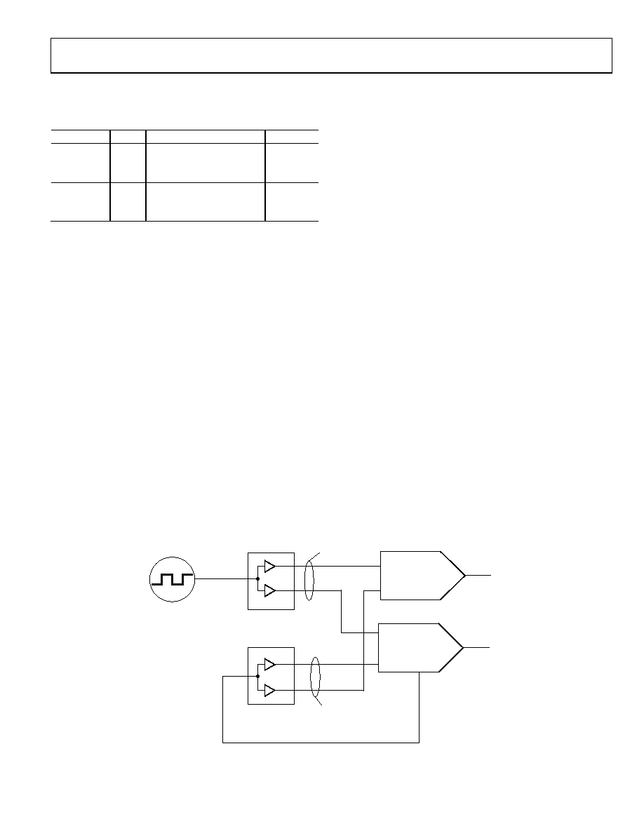
SYNCHRONIZING MULTIPLE DEVICES TO EACH
OTHER
The AD9785/AD9787/AD9788 synchronization engine uses
a PN code synchronization scheme to align multiple devices
within a system to the same DAC clock edge. The PN code
scheme synchronizes all the internal clocks, as well as the phase
accumulator of the NCO for all devices. With this scheme, one
device functions as the master, and the remainder of the devices
are configured as slaves.
The master device generates the PN encoded signal and drives
the signal out on the SYNC_O (SYNC_O+/SYNC_O) output
pins. This signal is then sent to the SYNC_I (SYNC_I+/
SYNC_I) inputs of all the slave devices and to itself. The slave
devices receive the code from the master and demodulate the
signal to produce a synchronization pulse every time a valid
code is received. The encoded signal of every device must be
sampled on the same DAC clock edge for the devices to be
properly synchronized. Therefore, it is extremely important that
the REFCLK signals arrive at all the devices with as little skew
between them as possible. In addition, the SYNC_I signals must
arrive at all the devices with as little skew as possible. At high
DACCLK frequencies, this requires using low skew clock
distribution devices to deliver the REFCLK and SYNC_I signals
and paying careful attention to printed circuit board signal
routing to equalize the trace lengths of these signals.
07
09
8-
1
03
SYSTEM CLOCK
LOW SKEW
CLOCK DRIVER
LOW SKEW
CLOCK DRIVER
MATCHED
LENGTH TRACES
MATCHED
LENGTH TRACES
REFCLK
TXENABLE
SYNC_I
REFCLK
TXENABLE
SYNC_I
OUT
SYNC_O
Figure 64. Multichip Synchronization in PN Code Mode
相关PDF资料 |
PDF描述 |
|---|---|
| EEM36DTMD-S189 | CONN EDGECARD 72POS R/A .156 SLD |
| EEM36DTMH-S189 | CONN EDGECARD 72POS R/A .156 SLD |
| 0210390421 | CABLE FLAT FLEX 1.18" 1MM 26POS |
| EVAL-AD5791SDZ | BOARD EVAL FOR AD5791 |
| VE-J2R-EZ | CONVERTER MOD DC/DC 7.5V 25W |
相关代理商/技术参数 |
参数描述 |
|---|---|
| AD9785-EBZ | 制造商:Analog Devices 功能描述:Evaluation Board For AD9785 制造商:Analog Devices 功能描述:DUAL 12B, 1GSPS D-A CONVERTER - Bulk 制造商:Analog Devices 功能描述:Digital to Analog Eval. Board |
| AD9786 | 制造商:AD 制造商全称:Analog Devices 功能描述:16-Bit, 200 MSPS/500 MSPS TxDAC+ with 2】/4】/8】 Interpolation and Signal Processing |
| AD9786BSV | 制造商:Analog Devices 功能描述:DAC 1-CH Interpolation Filter 16-bit 80-Pin TQFP EP 制造商:Analog Devices 功能描述:IC 16BIT DAC SMD 9786 TQFP80 |
| AD9786BSVRL | 制造商:Analog Devices 功能描述:DAC 1-CH Interpolation Filter 16-bit 80-Pin TQFP EP T/R |
| AD9786BSVZ | 功能描述:IC DAC 16BIT INTERPOL/SP 80TQFP RoHS:是 类别:集成电路 (IC) >> 数据采集 - 数模转换器 系列:TxDAC+® 标准包装:1 系列:- 设置时间:4.5µs 位数:12 数据接口:串行,SPI? 转换器数目:1 电压电源:单电源 功率耗散(最大):- 工作温度:-40°C ~ 125°C 安装类型:表面贴装 封装/外壳:8-SOIC(0.154",3.90mm 宽) 供应商设备封装:8-SOICN 包装:剪切带 (CT) 输出数目和类型:1 电压,单极;1 电压,双极 采样率(每秒):* 其它名称:MCP4921T-E/SNCTMCP4921T-E/SNRCTMCP4921T-E/SNRCT-ND |
发布紧急采购,3分钟左右您将得到回复。