- 您现在的位置:买卖IC网 > PDF目录19382 > ADSP-21161NCCAZ100 (Analog Devices Inc)IC DSP CONTROLLER 32BIT 225MBGA PDF资料下载
参数资料
| 型号: | ADSP-21161NCCAZ100 |
| 厂商: | Analog Devices Inc |
| 文件页数: | 20/60页 |
| 文件大小: | 0K |
| 描述: | IC DSP CONTROLLER 32BIT 225MBGA |
| 产品培训模块: | SHARC Processor Overview |
| 标准包装: | 1 |
| 系列: | SHARC® |
| 类型: | 浮点 |
| 接口: | 主机接口,连接端口,串行端口 |
| 时钟速率: | 100MHz |
| 非易失内存: | 外部 |
| 芯片上RAM: | 128kB |
| 电压 - 输入/输出: | 3.30V |
| 电压 - 核心: | 1.80V |
| 工作温度: | -40°C ~ 105°C |
| 安装类型: | 表面贴装 |
| 封装/外壳: | 225-BGA,CSPBGA |
| 供应商设备封装: | 225-CSPBGA(17x17) |
| 包装: | 托盘 |
| 其它名称: | ADSP21161NCCAZ100 |
第1页第2页第3页第4页第5页第6页第7页第8页第9页第10页第11页第12页第13页第14页第15页第16页第17页第18页第19页当前第20页第21页第22页第23页第24页第25页第26页第27页第28页第29页第30页第31页第32页第33页第34页第35页第36页第37页第38页第39页第40页第41页第42页第43页第44页第45页第46页第47页第48页第49页第50页第51页第52页第53页第54页第55页第56页第57页第58页第59页第60页
Rev. C
|
Page 27 of 60
|
January 2013
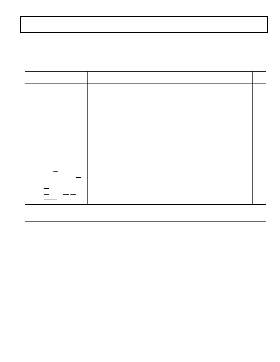
Memory Read — Bus Master
Use these specifications for asynchronous interfacing to memo-
ries (and memory-mapped peripherals) without reference to
CLKIN except for ACK pin requirements listed in footnote 4 of
Table 16. These specifications apply when the ADSP-21161N is
the bus master accessing external memory space in asynchro-
nous access mode.
Table 16. Memory Read — Bus Master
100 MHz
110 MHz
Parameter
Min
Max
Min
Max
Unit
Timing Requirements
tDAD
Address, Selects Delay to
Data Valid
tCKOP–0.25tCCLK–8.5+W
tCKOP–0.25tCCLK–6.75+W ns
tDRLD
RD Low to Data Valid1,3
0.75tCKOP–11+W
ns
tHDA
Data Hold from Address,
Selects
00ns
tSDS
Data Setup to RD High
88ns
tHDRH
Data Hold from RD High4 11ns
tDAAK
ACK Delay from Address,
Selects2, 5
tCKOP–0.5tCCLK–12+W
ns
tDSAK
ACK Delay from RD Low5
tCKOP–0.75tCCLK–11+W
ns
tSAKC
ACK Setup to CLKIN5
0.5tCCLK+3
ns
tHAKC
ACK Hold After CLKIN
1
ns
Switching Characteristics
tDRHA
Address Selects Hold
After RD High
0.25tCCLK–1+H
ns
tDARL
Address Selects to RD
0.25tCCLK–3
ns
tRW
RD Pulsewidth
tCKOP–0.5tCCLK–1+W
ns
tRWR
RD High to WR, RD,
DMAGx Low
0.5tCCLK–1+HI
ns
W = (number of wait states specified in WAIT register) × tCKOP.
HI = tCKOP (if an address hold cycle or bus idle cycle occurs, as specified in WAIT register; otherwise HI = 0).
H = tCKOP (if an address hold cycle occurs as specified in WAIT register; otherwise H = 0).
1 Data Delay/Setup: User must meet t
DAD, tDRLD, or tSDS.
2 The falling edge of MSx, BMS is referenced.
3 The maximum limits of timing requirement values for tDAD and tDRLD parameters are applicable for the case where ACK is always high.
4 Data Hold: User must meet t
HDA or tHDRH in asynchronous access mode. See Example System Hold Time Calculation on Page 54 for the calculation of hold times given capacitive
and dc loads.
5 For asynchronous access, ACK is sampled only after the programmed wait states for the access have been counted. For the first CLKIN cycle of a new external memory access,
ACK must be driven low (deasserted) by tDAAK, tDSAK, or tSAKC. For the second and subsequent cycles of an asynchronous external memory access, the tSAKC and tHAKC must be
met for both assertion and deassertion of ACK signal.
相关PDF资料 |
PDF描述 |
|---|---|
| VE-B1V-CV-F1 | CONVERTER MOD DC/DC 5.8V 150W |
| THJD107M010RJN | CAP TANT 100UF 10V 20% 2917 |
| VI-2NZ-CY-F3 | CONVERTER MOD DC/DC 2V 20W |
| 2300973 | CONN 37POS D-SUB W/SCREW |
| 1130-681K-RC | CHOKE RF HI CURR 680UH 10% RAD |
相关代理商/技术参数 |
参数描述 |
|---|---|
| ADSP-21161NKCA-100 | 功能描述:IC DSP CONTROLLER 32BIT 225MBGA RoHS:否 类别:集成电路 (IC) >> 嵌入式 - DSP(数字式信号处理器) 系列:SHARC® 标准包装:2 系列:StarCore 类型:SC140 内核 接口:DSI,以太网,RS-232 时钟速率:400MHz 非易失内存:外部 芯片上RAM:1.436MB 电压 - 输入/输出:3.30V 电压 - 核心:1.20V 工作温度:-40°C ~ 105°C 安装类型:表面贴装 封装/外壳:431-BFBGA,FCBGA 供应商设备封装:431-FCPBGA(20x20) 包装:托盘 |
| ADSP-21161NKCA-100Z | 制造商:Analog Devices 功能描述: |
| ADSP-21161NKCAZ100 | 功能描述:IC DSP CONTROLLER 32BIT 225MBGA RoHS:是 类别:集成电路 (IC) >> 嵌入式 - DSP(数字式信号处理器) 系列:SHARC® 标准包装:2 系列:StarCore 类型:SC140 内核 接口:DSI,以太网,RS-232 时钟速率:400MHz 非易失内存:外部 芯片上RAM:1.436MB 电压 - 输入/输出:3.30V 电压 - 核心:1.20V 工作温度:-40°C ~ 105°C 安装类型:表面贴装 封装/外壳:431-BFBGA,FCBGA 供应商设备封装:431-FCPBGA(20x20) 包装:托盘 |
| ADSP-21161NYCAZ110 | 功能描述:IC DSP CONTROLLER 32BIT 225BGA RoHS:是 类别:集成电路 (IC) >> 嵌入式 - DSP(数字式信号处理器) 系列:SHARC® 标准包装:2 系列:StarCore 类型:SC140 内核 接口:DSI,以太网,RS-232 时钟速率:400MHz 非易失内存:外部 芯片上RAM:1.436MB 电压 - 输入/输出:3.30V 电压 - 核心:1.20V 工作温度:-40°C ~ 105°C 安装类型:表面贴装 封装/外壳:431-BFBGA,FCBGA 供应商设备封装:431-FCPBGA(20x20) 包装:托盘 |
| ADSP-21261 | 制造商:AD 制造商全称:Analog Devices 功能描述:SHARC Embedded Processor |
发布紧急采购,3分钟左右您将得到回复。