- 您现在的位置:买卖IC网 > PDF目录19382 > ADSP-21161NCCAZ100 (Analog Devices Inc)IC DSP CONTROLLER 32BIT 225MBGA PDF资料下载
参数资料
| 型号: | ADSP-21161NCCAZ100 |
| 厂商: | Analog Devices Inc |
| 文件页数: | 3/60页 |
| 文件大小: | 0K |
| 描述: | IC DSP CONTROLLER 32BIT 225MBGA |
| 产品培训模块: | SHARC Processor Overview |
| 标准包装: | 1 |
| 系列: | SHARC® |
| 类型: | 浮点 |
| 接口: | 主机接口,连接端口,串行端口 |
| 时钟速率: | 100MHz |
| 非易失内存: | 外部 |
| 芯片上RAM: | 128kB |
| 电压 - 输入/输出: | 3.30V |
| 电压 - 核心: | 1.80V |
| 工作温度: | -40°C ~ 105°C |
| 安装类型: | 表面贴装 |
| 封装/外壳: | 225-BGA,CSPBGA |
| 供应商设备封装: | 225-CSPBGA(17x17) |
| 包装: | 托盘 |
| 其它名称: | ADSP21161NCCAZ100 |
第1页第2页当前第3页第4页第5页第6页第7页第8页第9页第10页第11页第12页第13页第14页第15页第16页第17页第18页第19页第20页第21页第22页第23页第24页第25页第26页第27页第28页第29页第30页第31页第32页第33页第34页第35页第36页第37页第38页第39页第40页第41页第42页第43页第44页第45页第46页第47页第48页第49页第50页第51页第52页第53页第54页第55页第56页第57页第58页第59页第60页
Rev. C
|
Page 11 of 60
|
January 2013
PIN FUNCTION DESCRIPTIONS
ADSP-21161N pin definitions are listed below. Inputs identified
as synchronous (S) must meet timing requirements with respect
to CLKIN (or with respect to TCK for TMS, TDI). Inputs iden-
tified as asynchronous (A) can be asserted asynchronously to
CLKIN (or to TCK for TRST). Tie or pull unused inputs to
VDDEXT or GND, except for the following:
ADDR23–0, DATA47–0, BRST, CLKOUT (Note: These
pins have a logic-level hold circuit enabled on the
ADSP-21161N DSP with ID2–0 = 00x.)
PA, ACK, RD, WR, DMARx, DMAGx, (ID2–0 = 00x)
(Note: These pins have a pull-up enabled on the
ADSP-21161N DSP with ID2–0 = 00x.)
LxCLK, LxACK, LxDAT7–0 (LxPDRDE = 0) (Note: See
Link Port Buffer Control Register Bit definitions in the
ADSP-21161N SHARC DSP Hardware Reference.)
DxA, DxB, SCLKx, SPICLK, MISO, MOSI, EMU,
TMS,TRST, TDI (Note: These pins have a pull-up.)
The following symbols appear in the Type column of Table 2:
A = Asynchronous, G = Ground, I = Input, O = Output,
P = Power Supply, S = Synchronous, (A/D) = Active Drive,
(O/D) = Open Drain, and T = Three-State (when SBTS is
asserted or when the ADSP-21161N is a bus slave).
Unlike previous SHARC processors, the ADSP-21161N con-
tains internal series resistance equivalent to 50 on all
input/output drivers except the CLKIN and XTAL pins.
Therefore, for traces longer than six inches, external series resis-
tors on control, data, clock, or frame sync pins are not required
to dampen reflections from transmission line effects for point-
to-point connections. However, for more complex networks
such as a star configuration, series termination is still
recommended.
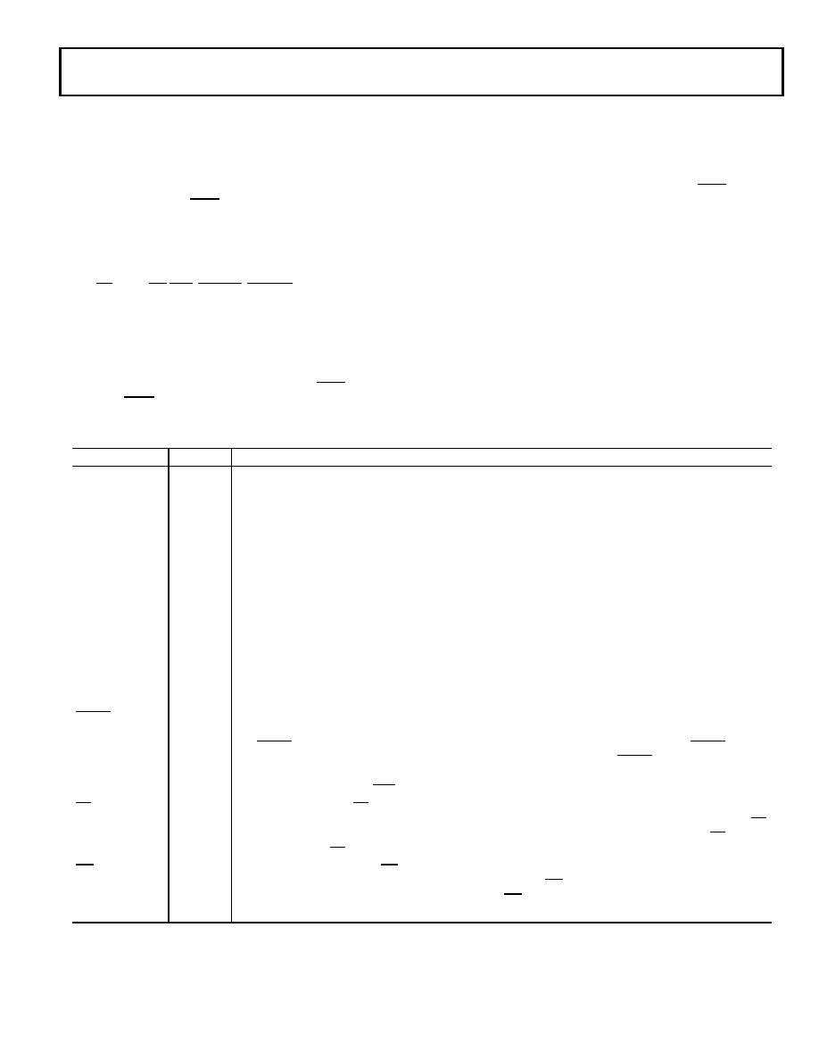
Table 2. Pin Function Descriptions
Pin
Type
Function
ADDR23–0
I/O/T
External Bus Address. The ADSP-21161N outputs addresses for external memory and peripherals on these
pins. In a multiprocessor system the bus master outputs addresses for read/writes of the IOP registers of other
ADSP-21161Ns while all other internal memory resources can be accessed indirectly via DMA control (that
is, accessing IOP DMA parameter registers). The ADSP-21161N inputs addresses when a host processor or
multiprocessing bus master is reading or writing its IOP registers. A keeper latch on the DSP’s ADDR23-0 pins
maintains the input at the level it was last driven. This latch is only enabled on the ADSP-21161N with
ID2–0=00x.
DATA47–16
I/O/T
External Bus Data. The ADSP-21161N inputs and outputs data and instructions on these pins. Pull-up
resistors on unused data pins are not necessary. A keeper latch on the DSP’s DATA47–16 pins maintains the
input at the level it was last driven. This latch is only enabled on the ADSP-21161N with ID2–0 =00x.
Note: DATA15–8 pins (multiplexed with L1DAT7–0) can also be used to extend the data bus if the link ports are
disabled and will not be used. In addition, DATA7–0 pins (multiplexed with L0DAT7–0) can also be used to extend
the data bus if the link ports are not used. This enables execution of 48-bit instructions from external SBSRAM
(system clock speed-external port), SRAM (system clock speed-external port) and SDRAM (core clock or one-half
the core clock speed). The IPACKx Instruction Packing Mode Bits in SYSCON should be set correctly (IPACK1–0 =0x1)
to enable this full instruction Width/No-packing Mode of operation.
MS3–0
I/O/T
Memory Select Lines. These outputs are asserted (low) as chip selects for the corresponding banks of
external memory. Memory bank sizes are fixed to 16 M words for non-SDRAM and 64M words for SDRAM.
The MS3–0 outputs are decoded memory address lines. In asynchronous access mode, the MS3–0 outputs
transition with the other address outputs. In synchronous access modes, the MS3–0 outputs assert with the
other address lines; however, they deassert after the first CLKIN cycle in which ACK is sampled asserted. In a
multiprocessor system, the MSx signals are tracked by slave SHARCs.
RD
I/O/T
Memory Read Strobe. RD is asserted whenever ADSP-21161N reads a word from external memory or from
the IOP registers of other ADSP-21161Ns. External devices, including other ADSP-21161Ns, must assert RD
for reading from a word of the ADSP-21161N IOP register memory. In a multiprocessing system, RD is driven
by the bus master. RD has a 20 k
internal pull-up resistor that is enabled for DSPs with ID2–0=00x.
WR
I/O/T
Memory Write Low Strobe. WR is asserted when ADSP-21161N writes a word to external memory or IOP
registers of other ADSP-21161Ns. External devices must assert WR for writing to ADSP-21161N IOP registers.
In a multiprocessing system, the bus master drives WR. WR has a 20 k
internal pull-up resistor that is enabled
for DSPs with ID2–0 =00x.
相关PDF资料 |
PDF描述 |
|---|---|
| VE-B1V-CV-F1 | CONVERTER MOD DC/DC 5.8V 150W |
| THJD107M010RJN | CAP TANT 100UF 10V 20% 2917 |
| VI-2NZ-CY-F3 | CONVERTER MOD DC/DC 2V 20W |
| 2300973 | CONN 37POS D-SUB W/SCREW |
| 1130-681K-RC | CHOKE RF HI CURR 680UH 10% RAD |
相关代理商/技术参数 |
参数描述 |
|---|---|
| ADSP-21161NKCA-100 | 功能描述:IC DSP CONTROLLER 32BIT 225MBGA RoHS:否 类别:集成电路 (IC) >> 嵌入式 - DSP(数字式信号处理器) 系列:SHARC® 标准包装:2 系列:StarCore 类型:SC140 内核 接口:DSI,以太网,RS-232 时钟速率:400MHz 非易失内存:外部 芯片上RAM:1.436MB 电压 - 输入/输出:3.30V 电压 - 核心:1.20V 工作温度:-40°C ~ 105°C 安装类型:表面贴装 封装/外壳:431-BFBGA,FCBGA 供应商设备封装:431-FCPBGA(20x20) 包装:托盘 |
| ADSP-21161NKCA-100Z | 制造商:Analog Devices 功能描述: |
| ADSP-21161NKCAZ100 | 功能描述:IC DSP CONTROLLER 32BIT 225MBGA RoHS:是 类别:集成电路 (IC) >> 嵌入式 - DSP(数字式信号处理器) 系列:SHARC® 标准包装:2 系列:StarCore 类型:SC140 内核 接口:DSI,以太网,RS-232 时钟速率:400MHz 非易失内存:外部 芯片上RAM:1.436MB 电压 - 输入/输出:3.30V 电压 - 核心:1.20V 工作温度:-40°C ~ 105°C 安装类型:表面贴装 封装/外壳:431-BFBGA,FCBGA 供应商设备封装:431-FCPBGA(20x20) 包装:托盘 |
| ADSP-21161NYCAZ110 | 功能描述:IC DSP CONTROLLER 32BIT 225BGA RoHS:是 类别:集成电路 (IC) >> 嵌入式 - DSP(数字式信号处理器) 系列:SHARC® 标准包装:2 系列:StarCore 类型:SC140 内核 接口:DSI,以太网,RS-232 时钟速率:400MHz 非易失内存:外部 芯片上RAM:1.436MB 电压 - 输入/输出:3.30V 电压 - 核心:1.20V 工作温度:-40°C ~ 105°C 安装类型:表面贴装 封装/外壳:431-BFBGA,FCBGA 供应商设备封装:431-FCPBGA(20x20) 包装:托盘 |
| ADSP-21261 | 制造商:AD 制造商全称:Analog Devices 功能描述:SHARC Embedded Processor |
发布紧急采购,3分钟左右您将得到回复。