- 您现在的位置:买卖IC网 > PDF目录19382 > ADSP-21161NCCAZ100 (Analog Devices Inc)IC DSP CONTROLLER 32BIT 225MBGA PDF资料下载
参数资料
| 型号: | ADSP-21161NCCAZ100 |
| 厂商: | Analog Devices Inc |
| 文件页数: | 32/60页 |
| 文件大小: | 0K |
| 描述: | IC DSP CONTROLLER 32BIT 225MBGA |
| 产品培训模块: | SHARC Processor Overview |
| 标准包装: | 1 |
| 系列: | SHARC® |
| 类型: | 浮点 |
| 接口: | 主机接口,连接端口,串行端口 |
| 时钟速率: | 100MHz |
| 非易失内存: | 外部 |
| 芯片上RAM: | 128kB |
| 电压 - 输入/输出: | 3.30V |
| 电压 - 核心: | 1.80V |
| 工作温度: | -40°C ~ 105°C |
| 安装类型: | 表面贴装 |
| 封装/外壳: | 225-BGA,CSPBGA |
| 供应商设备封装: | 225-CSPBGA(17x17) |
| 包装: | 托盘 |
| 其它名称: | ADSP21161NCCAZ100 |
第1页第2页第3页第4页第5页第6页第7页第8页第9页第10页第11页第12页第13页第14页第15页第16页第17页第18页第19页第20页第21页第22页第23页第24页第25页第26页第27页第28页第29页第30页第31页当前第32页第33页第34页第35页第36页第37页第38页第39页第40页第41页第42页第43页第44页第45页第46页第47页第48页第49页第50页第51页第52页第53页第54页第55页第56页第57页第58页第59页第60页
Rev. C
|
Page 38 of 60
|
January 2013
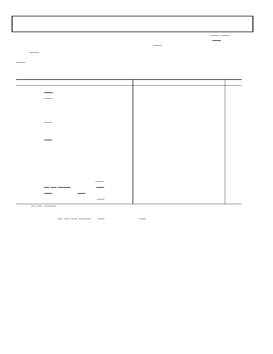
Three-State Timing — Bus Master, Bus Slave
These specifications show how the memory interface is disabled
(stops driving) or enabled (resumes driving) relative to CLKIN
and the SBTS pin. This timing is applicable to bus master transi-
tion cycles (BTC) and host transition cycles (HTC) as well as the
SBTS pin.
During reset, the DSP will not respond to SBTS, HBR, and MMS
accesses. Although the DSP will recognize HBR asserted before
reset, a HBG will not be returned by the DSP until after reset is
deasserted and the DSP completes bus synchronization.
Table 24. Three-State Timing — Bus Master, Bus Slave
Parameter
Min
Max
Unit
Timing Requirements
tSTSCK
SBTS Setup Before CLKIN
6
ns
tHTSCK
SBTS Hold After CLKIN
2
ns
Switching Characteristics
tMIENA
Address/Select Enable After CLKIN High
1.5
9
ns
tMIENS
Strobes Enable After CLKIN High1
–1.5
+9
ns
tMIENHG
HBG Enable After CLKIN
1.5
9
ns
tMITRA
Address/Select Disable After CLKIN High
0.5tCKOP–20
0.5tCKOP–15
ns
tMITRS
Strobes Disable After CLKIN High
tCKOP–0.25tCCLK–17
tCKOP–0.25tCCLK–12.5
ns
tMITRHG
HBG Disable After CLKIN
0.5tCKOP+NtCCLK–20
0.5tCKOP+NtCCLK–15
ns
tDATEN
Data Enable After CLKIN
1.5
10
ns
tDATTR
Data Disable After CLKIN3
1.5
6
ns
tACKEN
ACK Enable After CLKIN High
1.5
9
ns
tACKTR
ACK Disable After CLKIN High
0.2
5
ns
tCDCEN
CLKOUT Enable After CLKIN
0.5tCKOP+NtCCLK
0.5tCKOP+NtCCLK+5
ns
tCDCTR
CLKOUT Disable After CLKIN
tCKOP–5
tCKOP
ns
tATRHBG
Address/Select Disable Before HBG Low
1.5tCKOP–6
1.5tCKOP+2
ns
tSTRHBG
RD/WR/DMAGx Disable Before HBG Low
tCKOP+0.25tCCLK–4
tCKOP+0.25tCCLK+3
ns
tBTRHBG
BMS Disable Before HBG Low4
0.5tCKOP–4
0.5tCKOP+2
ns
tMENHBG
Memory Interface Enable After HBG High4
tCKOP–5
tCKOP+5
ns
1 Strobes = RD, WR, DMAGx.
2 Where N = 0.5, 1.0, 1.5 for 1:2, 1:3, and 1:4, respectively.
3 In addition to bus master transition cycles, these specs also apply to bus master and bus slave synchronous read/write.
4 Memory Interface = Address, RD, WR, MSx, DMAGx, and BMS (in EPROM boot mode). BMS is only an output in EPROM boot mode.
相关PDF资料 |
PDF描述 |
|---|---|
| VE-B1V-CV-F1 | CONVERTER MOD DC/DC 5.8V 150W |
| THJD107M010RJN | CAP TANT 100UF 10V 20% 2917 |
| VI-2NZ-CY-F3 | CONVERTER MOD DC/DC 2V 20W |
| 2300973 | CONN 37POS D-SUB W/SCREW |
| 1130-681K-RC | CHOKE RF HI CURR 680UH 10% RAD |
相关代理商/技术参数 |
参数描述 |
|---|---|
| ADSP-21161NKCA-100 | 功能描述:IC DSP CONTROLLER 32BIT 225MBGA RoHS:否 类别:集成电路 (IC) >> 嵌入式 - DSP(数字式信号处理器) 系列:SHARC® 标准包装:2 系列:StarCore 类型:SC140 内核 接口:DSI,以太网,RS-232 时钟速率:400MHz 非易失内存:外部 芯片上RAM:1.436MB 电压 - 输入/输出:3.30V 电压 - 核心:1.20V 工作温度:-40°C ~ 105°C 安装类型:表面贴装 封装/外壳:431-BFBGA,FCBGA 供应商设备封装:431-FCPBGA(20x20) 包装:托盘 |
| ADSP-21161NKCA-100Z | 制造商:Analog Devices 功能描述: |
| ADSP-21161NKCAZ100 | 功能描述:IC DSP CONTROLLER 32BIT 225MBGA RoHS:是 类别:集成电路 (IC) >> 嵌入式 - DSP(数字式信号处理器) 系列:SHARC® 标准包装:2 系列:StarCore 类型:SC140 内核 接口:DSI,以太网,RS-232 时钟速率:400MHz 非易失内存:外部 芯片上RAM:1.436MB 电压 - 输入/输出:3.30V 电压 - 核心:1.20V 工作温度:-40°C ~ 105°C 安装类型:表面贴装 封装/外壳:431-BFBGA,FCBGA 供应商设备封装:431-FCPBGA(20x20) 包装:托盘 |
| ADSP-21161NYCAZ110 | 功能描述:IC DSP CONTROLLER 32BIT 225BGA RoHS:是 类别:集成电路 (IC) >> 嵌入式 - DSP(数字式信号处理器) 系列:SHARC® 标准包装:2 系列:StarCore 类型:SC140 内核 接口:DSI,以太网,RS-232 时钟速率:400MHz 非易失内存:外部 芯片上RAM:1.436MB 电压 - 输入/输出:3.30V 电压 - 核心:1.20V 工作温度:-40°C ~ 105°C 安装类型:表面贴装 封装/外壳:431-BFBGA,FCBGA 供应商设备封装:431-FCPBGA(20x20) 包装:托盘 |
| ADSP-21261 | 制造商:AD 制造商全称:Analog Devices 功能描述:SHARC Embedded Processor |
发布紧急采购,3分钟左右您将得到回复。