- 您现在的位置:买卖IC网 > PDF目录19383 > ADSP-BF535PBBZ-200 (Analog Devices Inc)IC DSP CONTROLLER 16BIT 260-BGA PDF资料下载
参数资料
| 型号: | ADSP-BF535PBBZ-200 |
| 厂商: | Analog Devices Inc |
| 文件页数: | 31/44页 |
| 文件大小: | 0K |
| 描述: | IC DSP CONTROLLER 16BIT 260-BGA |
| 产品培训模块: | Blackfin® Processor Core Architecture Overview Blackfin® Device Drivers Blackfin® Optimizations for Performance and Power Consumption Blackfin® System Services |
| 标准包装: | 1 |
| 系列: | Blackfin® |
| 类型: | 定点 |
| 接口: | PCI,SPI,SSP,UART,USB |
| 时钟速率: | 200MHz |
| 非易失内存: | 外部 |
| 芯片上RAM: | 308kB |
| 电压 - 输入/输出: | 3.30V |
| 电压 - 核心: | 1.50V |
| 工作温度: | -40°C ~ 85°C |
| 安装类型: | 表面贴装 |
| 封装/外壳: | 260-BBGA |
| 供应商设备封装: | 260-PBGA(19x19) |
| 包装: | 托盘 |
第1页第2页第3页第4页第5页第6页第7页第8页第9页第10页第11页第12页第13页第14页第15页第16页第17页第18页第19页第20页第21页第22页第23页第24页第25页第26页第27页第28页第29页第30页当前第31页第32页第33页第34页第35页第36页第37页第38页第39页第40页第41页第42页第43页第44页
–37–
REV. A
ADSP-BF535
The frequency f includes driving the load high and then back low.
For example: DATA31–0 pins can drive high and low at a
maximum rate of 1/(2
tSCLK) while in SDRAM burst mode.
A typical power consumption can now be calculated for these
conditions by adding a typical internal power dissipation:
Note that the conditions causing a worst-case PEXT differ from
those causing a worst-case P
INT . Maximum PINT cannot occur
while 100% of the output pins are switching from all ones (1s) to
all zeros (0s). Note, as well, that it is not common for an appli-
cation to have 100% or even 50% of the outputs switching
simultaneously.
Test Conditions
All timing parameters appearing in this data sheet were measured
under the conditions described in this section.
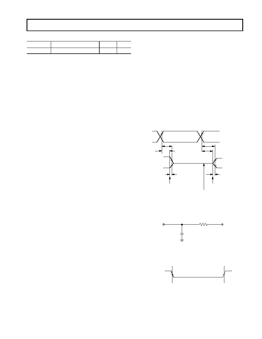
Output Enable Time
Output pins are considered to be enabled when they have made
a transition from a high impedance state to the point when they
start driving. The output enable time tENA is the interval from the
point when a reference signal reaches a high or low voltage level
to the point when the output starts driving as shown in the Output
the interval from when the reference signal switches to when the
output voltage reaches 2.0 V (output high) or 1.0 V (output low).
Time tTRIP is the interval from when the output starts driving to
when the output reaches the 1.0 V or 2.0 V trip voltage. Time
tENA is calculated as shown in the equation:
If multiple pins (such as the data bus) are enabled, the measure-
ment value is that of the first pin to start driving.
Output Disable Time
Output pins are considered to be disabled when they stop driving,
go into a high impedance state, and start to decay from their
output high or low voltage. The time for the voltage on the bus
to decay by
V is dependent on the capacitive load, C
L and the
load current, IL. This decay time can be approximated by the
equation:
The output disable time tDIS is the difference between
tDIS_MEASURED is the interval from when the reference signal
switches to when the output voltage decays
V from the measured
output high or output low voltage. The time tDECAY is calculated
with test loads CL and IL, and with
V equal to 0.5 V.
Example System Hold Time Calculation
To determine the data output hold time in a particular system,
first calculate tDECAY using the equation given above. Choose
V
to be the difference between the ADSP-BF535 Blackfin proces-
sor’s output voltage and the input threshold for the device
requiring the hold time. A typical
V will be 0.4 V. C
L is the total
bus capacitance (per data line), and IL is the total leakage or three-
state current (per data line). The hold time will be tDECAY plus the
minimum disable time (for example, tDSDAT for an SDRAM write
cycle).
Table 27. PLL Power Dissipation
Parameter
Test Conditions
Typical
Unit
IDDPLL
VDDPLL=1.5 V, 25C
4.0
mA
PTOTAL
PEXT
I
( DD VDDINT
×)
+
=
tENA tENA_MEASURED
=
tTRIP
–
tDECAY
CLV
() IL
=
Figure 22. Output Enable/Disable
Figure 23. Equivalent Device Loading for AC
Measurements (Includes All Fixtures)
Figure 24. Voltage Reference Levels for AC
Measurements (Except Output Enable/Disable)
REFERENCE
SIGNAL
tDIS
OUTPUT STARTS DRIVING
VOH (MEASURED)
V
VOL (MEASURED) + V
tDIS_MEASURED
VOH
(MEASURED)
VOL
(MEASURED)
2.0V
1.0V
VOH
(MEASURED)
VOL
(MEASURED)
HIGH IMPEDANCE STATE.
TEST CONDITIONS CAUSE THIS
VOLTAGE TO BE APPROXIMATELY 1.5V.
OUTPUT STOPS DRIVING
tENA
tDECAY
tENA-MEASURED
tTRIP
1.5V
30pF
TO
OUTPUT
PIN
50
INPUT
OR
OUTPUT
1.5V
相关PDF资料 |
PDF描述 |
|---|---|
| ADSP-21368KBPZ-2A | IC DSP 32BIT 333MHZ 256-BGA |
| MC79M15CT | IC REG LDO -15V .5A TO220AB |
| TLJR336M004R3000 | CAP TANT 33UF 4V 20% 0805 |
| VI-21T-CW-F4 | CONVERTER MOD DC/DC 6.5V 100W |
| MC79M12CT | IC REG LDO -12V .5A TO220AB |
相关代理商/技术参数 |
参数描述 |
|---|---|
| ADSPBF535PKB300 | 制造商:Analog Devices 功能描述: |
| ADSP-BF535PKB-300 | 功能描述:IC DSP CONTROLLER 16BIT 260 BGA RoHS:否 类别:集成电路 (IC) >> 嵌入式 - DSP(数字式信号处理器) 系列:Blackfin® 标准包装:2 系列:StarCore 类型:SC140 内核 接口:DSI,以太网,RS-232 时钟速率:400MHz 非易失内存:外部 芯片上RAM:1.436MB 电压 - 输入/输出:3.30V 电压 - 核心:1.20V 工作温度:-40°C ~ 105°C 安装类型:表面贴装 封装/外壳:431-BFBGA,FCBGA 供应商设备封装:431-FCPBGA(20x20) 包装:托盘 |
| ADSP-BF535PKB-350 | 功能描述:IC DSP CONTROLLER 16BIT 260 BGA RoHS:否 类别:集成电路 (IC) >> 嵌入式 - DSP(数字式信号处理器) 系列:Blackfin® 标准包装:2 系列:StarCore 类型:SC140 内核 接口:DSI,以太网,RS-232 时钟速率:400MHz 非易失内存:外部 芯片上RAM:1.436MB 电压 - 输入/输出:3.30V 电压 - 核心:1.20V 工作温度:-40°C ~ 105°C 安装类型:表面贴装 封装/外壳:431-BFBGA,FCBGA 供应商设备封装:431-FCPBGA(20x20) 包装:托盘 |
| ADSP-BF535PKB-C91 | 制造商:Analog Devices 功能描述: |
| ADSP-BF535PKBZ-300 | 功能描述:IC DSP CONTROLLER 16BIT 260 BGA RoHS:是 类别:集成电路 (IC) >> 嵌入式 - DSP(数字式信号处理器) 系列:Blackfin® 标准包装:40 系列:TMS320DM64x, DaVinci™ 类型:定点 接口:I²C,McASP,McBSP 时钟速率:400MHz 非易失内存:外部 芯片上RAM:160kB 电压 - 输入/输出:3.30V 电压 - 核心:1.20V 工作温度:0°C ~ 90°C 安装类型:表面贴装 封装/外壳:548-BBGA,FCBGA 供应商设备封装:548-FCBGA(27x27) 包装:托盘 配用:TMDSDMK642-0E-ND - DEVELPER KIT W/NTSC CAMERA296-23038-ND - DSP STARTER KIT FOR TMS320C6416296-23059-ND - FLASHBURN PORTING KIT296-23058-ND - EVAL MODULE FOR DM642TMDSDMK642-ND - DEVELOPER KIT W/NTSC CAMERA |
发布紧急采购,3分钟左右您将得到回复。