- 您现在的位置:买卖IC网 > PDF目录19383 > ADSP-BF535PBBZ-200 (Analog Devices Inc)IC DSP CONTROLLER 16BIT 260-BGA PDF资料下载
参数资料
| 型号: | ADSP-BF535PBBZ-200 |
| 厂商: | Analog Devices Inc |
| 文件页数: | 5/44页 |
| 文件大小: | 0K |
| 描述: | IC DSP CONTROLLER 16BIT 260-BGA |
| 产品培训模块: | Blackfin® Processor Core Architecture Overview Blackfin® Device Drivers Blackfin® Optimizations for Performance and Power Consumption Blackfin® System Services |
| 标准包装: | 1 |
| 系列: | Blackfin® |
| 类型: | 定点 |
| 接口: | PCI,SPI,SSP,UART,USB |
| 时钟速率: | 200MHz |
| 非易失内存: | 外部 |
| 芯片上RAM: | 308kB |
| 电压 - 输入/输出: | 3.30V |
| 电压 - 核心: | 1.50V |
| 工作温度: | -40°C ~ 85°C |
| 安装类型: | 表面贴装 |
| 封装/外壳: | 260-BBGA |
| 供应商设备封装: | 260-PBGA(19x19) |
| 包装: | 托盘 |
第1页第2页第3页第4页当前第5页第6页第7页第8页第9页第10页第11页第12页第13页第14页第15页第16页第17页第18页第19页第20页第21页第22页第23页第24页第25页第26页第27页第28页第29页第30页第31页第32页第33页第34页第35页第36页第37页第38页第39页第40页第41页第42页第43页第44页
–13–
REV. A
ADSP-BF535
The power dissipated by a processor is largely a function of the
clock frequency of the processor and the square of the operating
voltage. For example, reducing the clock frequency by 25%
results in a 25% reduction in power dissipation, while reducing
the voltage by 25% reduces power dissipation by more than 40%.
Further, these power savings are additive, in that if the clock
frequency and power are both reduced, the power savings are
dramatic.
Dynamic Power Management allows both the processor’s input
voltage (VDDINT) and clock frequency (fCCLK) to be dynamically
and independently controlled.
As previously explained, the savings in power dissipation can be
modeled by the following equation:
where:
is the nominal core clock frequency (300 MHz)
is the reduced core clock frequency
is the nominal internal supply voltage (1.5 V)
is the reduced internal supply voltage
As an example of how significant the power savings of Dynamic
Power Management are when both frequency and voltage are
reduced, consider an example where the frequency is reduced
from its nominal value to 50 MHz and the voltage is reduced from
its nominal value to 1.2 V. At this reduced frequency and voltage,
the processor dissipates about 10% of the power dissipated at
nominal frequency and voltage.
Peripheral Power Control
The ADSP-BF535 Blackfin processor provides additional power
control capability by allowing dynamic scheduling of clock inputs
to each of the peripherals. Clocking to each of the peripherals
listed below can be enabled or disabled by appropriately setting
the peripheral’s control bit in the peripheral clock enable register
(PLL_IOCK). The Peripheral Clock Enable Register allows indi-
vidual control for each of these peripherals:
PCI
EBIU controller
Programmable flags
MemDMA controller
SPORT 0
SPORT 1
SPI 0
SPI 1
UART 0
UART 1
Timer 0, Timer 1, Timer 2
USB CLK
Clock Signals
The ADSP-BF535 Blackfin processor can be clocked by a sine
wave input or a buffered shaped clock derived from an external
clock oscillator.
If a buffered, shaped clock is used, this external clock connects
to the processor CLKIN pin. The CLKIN input cannot be
halted, changed, or operated below the specified frequency
during normal operation. This clock signal should be a 3.3 V
LVTTL compatible signal. The processor provides a user-pro-
grammable 1
to 31
multiplication of the input clock to
support external-to-internal clock ratios. The MSEL6–0,
BYPASS, and DF pins decide the PLL multiplication factor at
reset. At run time, the multiplication factor can be controlled in
software. The combination of pull-up and pull-down resistors in
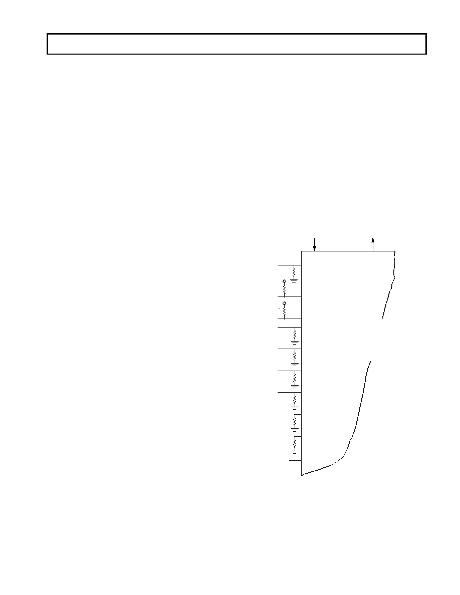
Figure 7 sets up a core clock ratio of 6:1, which, for example,
produces a 150 MHz core clock from the 25 MHz input. For
other clock multiplier settings, see the ADSP-BF535 Blackfin
Processor Hardware Reference.
All on-chip peripherals operate at the rate set by the system clock
(SCLK). The system clock frequency is programmable by means
of the SSEL pins. At run time the system clock frequency can be
controlled in software by writing to the SSEL fields in the PLL
control register (PLL_CTL). The values programmed into the
Power Dissipation Factor
fCCLKRED
fCCLKNOM
--------------------------
VDDINTRED
VDDINTNOM
------------------------------
2
×
=
fCCLKNOM
fCCLKRED
VDDINTNOM
VDDINTRED
Figure 7. Clock Ratio Example
CLKIN
CLKOUT
ADSP-BF535
MSEL5 (PF5)
MSEL4 (PF4)
MSEL3 (PF3)
MSEL2 (PF2)
MSEL1 (PF1)
MSEL0 (PF0)
RESET
MSEL6 (PF6)
DF (PF7)
VDD
BYPASS
RESET SOURCE
THE PULL-UP/PULL-DOWN
RESISTORS ON THE MSEL,
DF, AND BYPASS PINS SELECT
THE CORE CLOCK RATIO.
HERE, THE SELECTION (6:1)
AND 25MHz INPUT CLOCK
PRODUCE A 150MHz CORE CLOCK.
BLACKFIN PROCESSOR
VDD
相关PDF资料 |
PDF描述 |
|---|---|
| ADSP-21368KBPZ-2A | IC DSP 32BIT 333MHZ 256-BGA |
| MC79M15CT | IC REG LDO -15V .5A TO220AB |
| TLJR336M004R3000 | CAP TANT 33UF 4V 20% 0805 |
| VI-21T-CW-F4 | CONVERTER MOD DC/DC 6.5V 100W |
| MC79M12CT | IC REG LDO -12V .5A TO220AB |
相关代理商/技术参数 |
参数描述 |
|---|---|
| ADSPBF535PKB300 | 制造商:Analog Devices 功能描述: |
| ADSP-BF535PKB-300 | 功能描述:IC DSP CONTROLLER 16BIT 260 BGA RoHS:否 类别:集成电路 (IC) >> 嵌入式 - DSP(数字式信号处理器) 系列:Blackfin® 标准包装:2 系列:StarCore 类型:SC140 内核 接口:DSI,以太网,RS-232 时钟速率:400MHz 非易失内存:外部 芯片上RAM:1.436MB 电压 - 输入/输出:3.30V 电压 - 核心:1.20V 工作温度:-40°C ~ 105°C 安装类型:表面贴装 封装/外壳:431-BFBGA,FCBGA 供应商设备封装:431-FCPBGA(20x20) 包装:托盘 |
| ADSP-BF535PKB-350 | 功能描述:IC DSP CONTROLLER 16BIT 260 BGA RoHS:否 类别:集成电路 (IC) >> 嵌入式 - DSP(数字式信号处理器) 系列:Blackfin® 标准包装:2 系列:StarCore 类型:SC140 内核 接口:DSI,以太网,RS-232 时钟速率:400MHz 非易失内存:外部 芯片上RAM:1.436MB 电压 - 输入/输出:3.30V 电压 - 核心:1.20V 工作温度:-40°C ~ 105°C 安装类型:表面贴装 封装/外壳:431-BFBGA,FCBGA 供应商设备封装:431-FCPBGA(20x20) 包装:托盘 |
| ADSP-BF535PKB-C91 | 制造商:Analog Devices 功能描述: |
| ADSP-BF535PKBZ-300 | 功能描述:IC DSP CONTROLLER 16BIT 260 BGA RoHS:是 类别:集成电路 (IC) >> 嵌入式 - DSP(数字式信号处理器) 系列:Blackfin® 标准包装:40 系列:TMS320DM64x, DaVinci™ 类型:定点 接口:I²C,McASP,McBSP 时钟速率:400MHz 非易失内存:外部 芯片上RAM:160kB 电压 - 输入/输出:3.30V 电压 - 核心:1.20V 工作温度:0°C ~ 90°C 安装类型:表面贴装 封装/外壳:548-BBGA,FCBGA 供应商设备封装:548-FCBGA(27x27) 包装:托盘 配用:TMDSDMK642-0E-ND - DEVELPER KIT W/NTSC CAMERA296-23038-ND - DSP STARTER KIT FOR TMS320C6416296-23059-ND - FLASHBURN PORTING KIT296-23058-ND - EVAL MODULE FOR DM642TMDSDMK642-ND - DEVELOPER KIT W/NTSC CAMERA |
发布紧急采购,3分钟左右您将得到回复。