- 您现在的位置:买卖IC网 > PDF目录12027 > ADUC7021BCPZ62 (Analog Devices Inc)IC MCU FLSH 62K ANLG I/O 40LFCSP PDF资料下载
参数资料
| 型号: | ADUC7021BCPZ62 |
| 厂商: | Analog Devices Inc |
| 文件页数: | 32/104页 |
| 文件大小: | 0K |
| 描述: | IC MCU FLSH 62K ANLG I/O 40LFCSP |
| 产品培训模块: | ARM7 Applications & Tools Process Control |
| 标准包装: | 1 |
| 系列: | MicroConverter® ADuC7xxx |
| 核心处理器: | ARM7 |
| 芯体尺寸: | 16/32-位 |
| 速度: | 44MHz |
| 连通性: | EBI/EMI,I²C,SPI,UART/USART |
| 外围设备: | PLA,PWM,PSM,温度传感器,WDT |
| 输入/输出数: | 13 |
| 程序存储器容量: | 64KB(32K x 16) |
| 程序存储器类型: | 闪存 |
| RAM 容量: | 2K x 32 |
| 电压 - 电源 (Vcc/Vdd): | 2.7 V ~ 3.6 V |
| 数据转换器: | A/D 8x12b,D/A 2x12b |
| 振荡器型: | 内部 |
| 工作温度: | -40°C ~ 125°C |
| 封装/外壳: | 40-VFQFN 裸露焊盘,CSP |
| 包装: | 托盘 |
第1页第2页第3页第4页第5页第6页第7页第8页第9页第10页第11页第12页第13页第14页第15页第16页第17页第18页第19页第20页第21页第22页第23页第24页第25页第26页第27页第28页第29页第30页第31页当前第32页第33页第34页第35页第36页第37页第38页第39页第40页第41页第42页第43页第44页第45页第46页第47页第48页第49页第50页第51页第52页第53页第54页第55页第56页第57页第58页第59页第60页第61页第62页第63页第64页第65页第66页第67页第68页第69页第70页第71页第72页第73页第74页第75页第76页第77页第78页第79页第80页第81页第82页第83页第84页第85页第86页第87页第88页第89页第90页第91页第92页第93页第94页第95页第96页第97页第98页第99页第100页第101页第102页第103页第104页
Data Sheet
ADuC7019/20/21/22/24/25/26/27/28/29
Rev. F | Page 33 of 104
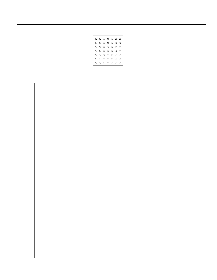
ADUC7029
BOTTOM VIEW
(Not to Scale)
7
4
5
6
3
2
1
A
B
C
D
E
F
G
04955-
088
Figure 27. 49-Ball CSP_BGA Pin Configuration (ADuC7029)
Table 15. Pin Function Descriptions (ADuC7029)
Ball No.
Mnemonic
Description
A1
ADC3/CMP1
Single-Ended or Differential Analog Input 3/Comparator Negative Input.
A2
ADC1
Single-Ended or Differential Analog Input 1.
A3
ADC0
Single-Ended or Differential Analog Input 0.
A4
AVDD
3.3 V Analog Power.
A5
VREF
2.5 V Internal Voltage Reference. Must be connected to a 0.47 F capacitor when using the
internal reference.
A6
P1.0/T1/SPM0/PLAI[0]
Serial Port Multiplexed. General-Purpose Input and Output Port 1.0/Timer1 Input/UART, I2C0/
Programmable Logic Array Input Element 0.
A7
P1.1/SPM1/PLAI[1]
Serial Port Multiplexed. General-Purpose Input and Output Port 1.1/UART, I2C0/Programmable
Logic Array Input Element 1.
B1
ADC6
Single-Ended or Differential Analog Input 6.
B2
ADC5
Single-Ended or Differential Analog Input 5.
B3
ADC4
Single-Ended or Differential Analog Input 4.
B4
AGND
Analog Ground. Ground reference point for the analog circuitry.
B5
DACREF
External Voltage Reference for the DACs. Range: DACGND to DACVDD.
B6
P1.4/SPM4/PLAI[4]/IRQ2
Serial Port Multiplexed. General-Purpose Input and Output Port 1.4/UART, SPI/Programmable
Logic Array Input Element 4/External Interrupt Request 2, Active High.
B7
P1.3/SPM3/PLAI[3]
Serial Port Multiplexed. General-Purpose Input and Output Port 1.3/UART, I2C1/Programmable
Logic Array Input Element 3.
C1
GNDREF
Ground Voltage Reference for the ADC. For optimal performance, the analog power supply
should be separated from IOGND and DGND.
C2
AGND
Analog Ground. Ground reference point for the analog circuitry.
C3
ADC2/CMP0
Single-Ended or Differential Analog Input 2/Comparator Positive Input.
C4
IOGND
Ground for GPIO (see Table 78). Typically connected to DGND.
C5
P1.2/SPM2/PLAI[2]
Serial Port Multiplexed. General-Purpose Input and Output Port 1.2/UART, I2C1/Programmable
Logic Array Input Element 2.
C6
P1.6/SPM6/PLAI[6]
Serial Port Multiplexed. General-Purpose Input and Output Port 1.6/UART, SPI/Programmable
Logic Array Input Element 6.
C7
P1.5/SPM5/PLAI[5]/IRQ3
Serial Port Multiplexed. General-Purpose Input and Output Port 1.5/UART, SPI/Programmable
Logic Array Input Element 5/External Interrupt Request 3, Active High.
D1
DAC0/ADC12
DAC0 Voltage Output/ADC Input 12.
D2
DAC3/ADC15
DAC3 Voltage Output/ADC Input 15.
D3
DAC1/ADC13
DAC1 Voltage Output/ADC Input 13.
D4
P3.3/PWM1L/PLAI[11]
General-Purpose Input and Output Port 3.3/PWM Phase 1 Low-Side Output/Programmable
Logic Array Input Element 11.
D5
P3.4/PWM2H/PLAI[12]
General-Purpose Input and Output Port 3.4/PWM Phase 2 High-Side Output/Programmable
Logic Array Input 12.
D6
P3.6/PWMTRIP/PLAI[14]
General-Purpose Input and Output Port 3.6/PWM Safety Cutoff/Programmable Logic Array
Input Element 14.
D7
P1.7/SPM7/PLAO[0]
Serial Port Multiplexed. General-Purpose Input and Output Port 1.7/UART, SPI/Programmable
Logic Array Output Element 0.
相关PDF资料 |
PDF描述 |
|---|---|
| VI-B2M-IY-F3 | CONVERTER MOD DC/DC 10V 50W |
| MUSB-2A111-024BP | DUST COVER FOR MUSB TYPE A BLACK |
| VI-B2M-IY-F2 | CONVERTER MOD DC/DC 10V 50W |
| AT89C51AC3-S3SUM | IC 8051 MCU 64K FLASH 52-PLCC |
| VI-B2M-IY-F1 | CONVERTER MOD DC/DC 10V 50W |
相关代理商/技术参数 |
参数描述 |
|---|---|
| ADUC7021BCPZ62I | 功能描述:IC MCU FLSH 62K ANLG I/O 40LFCSP RoHS:是 类别:集成电路 (IC) >> 嵌入式 - 微控制器, 系列:MicroConverter® ADuC7xxx 产品培训模块:MCU Product Line Introduction XMEGA Introduction AVR XMEGA USB Connectivity 标准包装:90 系列:AVR® XMEGA 核心处理器:AVR 芯体尺寸:8/16-位 速度:32MHz 连通性:I²C,IrDA,SPI,UART/USART 外围设备:欠压检测/复位,DMA,POR,PWM,WDT 输入/输出数:50 程序存储器容量:192KB(96K x 16) 程序存储器类型:闪存 EEPROM 大小:4K x 8 RAM 容量:16K x 8 电压 - 电源 (Vcc/Vdd):1.6 V ~ 3.6 V 数据转换器:A/D 16x12b; D/A 2x12b 振荡器型:内部 工作温度:-40°C ~ 85°C 封装/外壳:64-TQFP 包装:托盘 配用:ATSTK600-RC14-ND - STK600 SOCKET/ADAPTER 64TQFPATSTK600-TQFP64-ND - STK600 SOCKET/ADAPTER 64-TQFPATAVRONEKIT-ND - KIT AVR/AVR32 DEBUGGER/PROGRMMRATAVRISP2-ND - PROGRAMMER AVR IN SYSTEM |
| ADUC7021BCPZ62I-RL | 功能描述:IC MCU 12BIT 1MSPS I2C 40-LFCSP RoHS:是 类别:集成电路 (IC) >> 嵌入式 - 微控制器, 系列:MicroConverter® ADuC7xxx 标准包装:38 系列:Encore!® XP® 核心处理器:eZ8 芯体尺寸:8-位 速度:5MHz 连通性:IrDA,UART/USART 外围设备:欠压检测/复位,LED,POR,PWM,WDT 输入/输出数:16 程序存储器容量:4KB(4K x 8) 程序存储器类型:闪存 EEPROM 大小:- RAM 容量:1K x 8 电压 - 电源 (Vcc/Vdd):2.7 V ~ 3.6 V 数据转换器:- 振荡器型:内部 工作温度:-40°C ~ 105°C 封装/外壳:20-SOIC(0.295",7.50mm 宽) 包装:管件 其它名称:269-4116Z8F0413SH005EG-ND |
| ADUC7021BCPZ62IRL7 | 制造商:Analog Devices 功能描述:MCU 16-bit/32-bit ADuC7xxx ARM7TDMI RISC 62KB Flash 3.3V 40-Pin LFCSP EP T/R |
| ADUC7021BCPZ62-RL | 功能描述:IC MCU 12BIT 1MSPS UART 40-LFCSP RoHS:是 类别:集成电路 (IC) >> 嵌入式 - 微控制器, 系列:MicroConverter® ADuC7xxx 标准包装:38 系列:Encore!® XP® 核心处理器:eZ8 芯体尺寸:8-位 速度:5MHz 连通性:IrDA,UART/USART 外围设备:欠压检测/复位,LED,POR,PWM,WDT 输入/输出数:16 程序存储器容量:4KB(4K x 8) 程序存储器类型:闪存 EEPROM 大小:- RAM 容量:1K x 8 电压 - 电源 (Vcc/Vdd):2.7 V ~ 3.6 V 数据转换器:- 振荡器型:内部 工作温度:-40°C ~ 105°C 封装/外壳:20-SOIC(0.295",7.50mm 宽) 包装:管件 其它名称:269-4116Z8F0413SH005EG-ND |
| ADUC7021BCPZ62-RL7 | 功能描述:IC MCU 12BIT 1MSPS UART 40-LFCSP RoHS:是 类别:集成电路 (IC) >> 嵌入式 - 微控制器, 系列:MicroConverter® ADuC7xxx 标准包装:38 系列:Encore!® XP® 核心处理器:eZ8 芯体尺寸:8-位 速度:5MHz 连通性:IrDA,UART/USART 外围设备:欠压检测/复位,LED,POR,PWM,WDT 输入/输出数:16 程序存储器容量:4KB(4K x 8) 程序存储器类型:闪存 EEPROM 大小:- RAM 容量:1K x 8 电压 - 电源 (Vcc/Vdd):2.7 V ~ 3.6 V 数据转换器:- 振荡器型:内部 工作温度:-40°C ~ 105°C 封装/外壳:20-SOIC(0.295",7.50mm 宽) 包装:管件 其它名称:269-4116Z8F0413SH005EG-ND |
发布紧急采购,3分钟左右您将得到回复。