- 您现在的位置:买卖IC网 > PDF目录12027 > ADUC7021BCPZ62 (Analog Devices Inc)IC MCU FLSH 62K ANLG I/O 40LFCSP PDF资料下载
参数资料
| 型号: | ADUC7021BCPZ62 |
| 厂商: | Analog Devices Inc |
| 文件页数: | 88/104页 |
| 文件大小: | 0K |
| 描述: | IC MCU FLSH 62K ANLG I/O 40LFCSP |
| 产品培训模块: | ARM7 Applications & Tools Process Control |
| 标准包装: | 1 |
| 系列: | MicroConverter® ADuC7xxx |
| 核心处理器: | ARM7 |
| 芯体尺寸: | 16/32-位 |
| 速度: | 44MHz |
| 连通性: | EBI/EMI,I²C,SPI,UART/USART |
| 外围设备: | PLA,PWM,PSM,温度传感器,WDT |
| 输入/输出数: | 13 |
| 程序存储器容量: | 64KB(32K x 16) |
| 程序存储器类型: | 闪存 |
| RAM 容量: | 2K x 32 |
| 电压 - 电源 (Vcc/Vdd): | 2.7 V ~ 3.6 V |
| 数据转换器: | A/D 8x12b,D/A 2x12b |
| 振荡器型: | 内部 |
| 工作温度: | -40°C ~ 125°C |
| 封装/外壳: | 40-VFQFN 裸露焊盘,CSP |
| 包装: | 托盘 |
第1页第2页第3页第4页第5页第6页第7页第8页第9页第10页第11页第12页第13页第14页第15页第16页第17页第18页第19页第20页第21页第22页第23页第24页第25页第26页第27页第28页第29页第30页第31页第32页第33页第34页第35页第36页第37页第38页第39页第40页第41页第42页第43页第44页第45页第46页第47页第48页第49页第50页第51页第52页第53页第54页第55页第56页第57页第58页第59页第60页第61页第62页第63页第64页第65页第66页第67页第68页第69页第70页第71页第72页第73页第74页第75页第76页第77页第78页第79页第80页第81页第82页第83页第84页第85页第86页第87页当前第88页第89页第90页第91页第92页第93页第94页第95页第96页第97页第98页第99页第100页第101页第102页第103页第104页
ADuC7019/20/21/22/24/25/26/27/28/29
Data Sheet
Rev. F | Page 84 of 104
FIQ
The fast interrupt request (FIQ) is the exception signal to enter
the FIQ mode of the processor. It is provided to service data
transfer or communication channel tasks with low latency. The
FIQ interface is identical to the IRQ interface providing the
second-level interrupt (highest priority). Four 32-bit registers
are dedicated to FIQ: FIQSIG, FIQEN, FIQCLR, and FIQSTA.
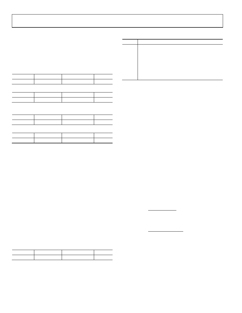
Table 165. FIQSTA Register
Name
Address
Default Value
Access
FIQSTA
0xFFFF0100
0x00000000
R
Table 166. FIQSIG Register
Name
Address
Default Value
Access
FIQSIG
0xFFFF0104
0x00XXX0001
R
1
X indicates an undefined value.
Table 167. FIQEN Register
Name
Address
Default Value
Access
FIQEN
0xFFFF0108
0x00000000
R/W
Table 168. FIQCLR Register
Name
Address
Default Value
Access
FIQCLR
0xFFFF010C
0x00000000
W
Bit 31 to Bit 1 of FIQSTA are logically OR’d to create the FIQ
signal to the core and to Bit 0 of both the FIQ and IRQ registers
(FIQ source).
The logic for FIQEN and IRQEN does not allow an interrupt
source to be enabled in both IRQ and FIQ masks. A bit set to 1
in FIQEN does, as a side effect, clear the same bit in IRQEN.
Also, a bit set to 1 in IRQEN does, as a side effect, clear the
same bit in FIQEN. An interrupt source can be disabled in both
the IRQEN and FIQEN masks.
Note that to clear an already enabled FIQ source, the user must
set the appropriate bit in the FIQCLR register. Clearing an
interrupt’s FIQEN bit does not disable the interrupt.
Programmed Interrupts
Because the programmed interrupts are nonmaskable, they are
controlled by another register, SWICFG, which simultaneously
writes into the IRQSTA and IRQSIG registers and/or the
FIQSTA and FIQSIG registers. The 32-bit SWICFG register is
dedicated to software interrupts(see Table 170). This MMR
allows the control of a programmed source interrupt.
Table 169. SWICFG Register
Name
Address
Default Value
Access
SWICFG
0xFFFF0010
0x00000000
W
Table 170. SWICFG MMR Bit Descriptions
Bit
Description
31:3
Reserved.
2
Programmed interrupt (FIQ). Setting/clearing this bit
corresponds with setting/clearing Bit 1 of FIQSTA
and FIQSIG.
1
Programmed interrupt (IRQ). Setting/clearing this bit
corresponds with setting/clearing Bit 1 of IRQSTA
and IRQSIG.
0
Reserved.
Note that any interrupt signal must be active for at least the
equivalent of the interrupt latency time, which is detected by
the interrupt controller and by the user in the IRQSTA/FIQSTA
register.
TIMERS
The ADuC7019/20/21/22/24/25/26/27/28/29 have four general-
purpose timer/counters.
Timer0
Timer1
Timer2 or wake-up timer
Timer3 or watchdog timer
These four timers in their normal mode of operation can be
either free running or periodic.
In free-running mode, the counter decreases from the
maximum value until zero scale and starts again at the
minimum value. (It also increases from the minimum value
until full scale and starts again at the maximum value.)
In periodic mode, the counter decrements/increments from the
value in the load register (TxLD MMR) until zero/full scale and
starts again at the value stored in the load register.
The timer interval is calculated as follows:
If the timer is set to count down then
(
)
Clock
Source
Prescaler
TxLD
Interval
×
=
If the timer is set to count up, then
(
)
Clock
Source
Prescaler
TxLD
Fs
Interval
×
=
The value of a counter can be read at any time by accessing its
value register (TxVAL). Note that when a timer is being clocked
from a clock other than core clock, an incorrect value may be
read (due to an asynchronous clock system). In this configur-
ation, TxVAL should always be read twice. If the two readings
are different, it should be read a third time to get the correct
value.
Timers are started by writing in the control register of the
corresponding timer (TxCON).
相关PDF资料 |
PDF描述 |
|---|---|
| VI-B2M-IY-F3 | CONVERTER MOD DC/DC 10V 50W |
| MUSB-2A111-024BP | DUST COVER FOR MUSB TYPE A BLACK |
| VI-B2M-IY-F2 | CONVERTER MOD DC/DC 10V 50W |
| AT89C51AC3-S3SUM | IC 8051 MCU 64K FLASH 52-PLCC |
| VI-B2M-IY-F1 | CONVERTER MOD DC/DC 10V 50W |
相关代理商/技术参数 |
参数描述 |
|---|---|
| ADUC7021BCPZ62I | 功能描述:IC MCU FLSH 62K ANLG I/O 40LFCSP RoHS:是 类别:集成电路 (IC) >> 嵌入式 - 微控制器, 系列:MicroConverter® ADuC7xxx 产品培训模块:MCU Product Line Introduction XMEGA Introduction AVR XMEGA USB Connectivity 标准包装:90 系列:AVR® XMEGA 核心处理器:AVR 芯体尺寸:8/16-位 速度:32MHz 连通性:I²C,IrDA,SPI,UART/USART 外围设备:欠压检测/复位,DMA,POR,PWM,WDT 输入/输出数:50 程序存储器容量:192KB(96K x 16) 程序存储器类型:闪存 EEPROM 大小:4K x 8 RAM 容量:16K x 8 电压 - 电源 (Vcc/Vdd):1.6 V ~ 3.6 V 数据转换器:A/D 16x12b; D/A 2x12b 振荡器型:内部 工作温度:-40°C ~ 85°C 封装/外壳:64-TQFP 包装:托盘 配用:ATSTK600-RC14-ND - STK600 SOCKET/ADAPTER 64TQFPATSTK600-TQFP64-ND - STK600 SOCKET/ADAPTER 64-TQFPATAVRONEKIT-ND - KIT AVR/AVR32 DEBUGGER/PROGRMMRATAVRISP2-ND - PROGRAMMER AVR IN SYSTEM |
| ADUC7021BCPZ62I-RL | 功能描述:IC MCU 12BIT 1MSPS I2C 40-LFCSP RoHS:是 类别:集成电路 (IC) >> 嵌入式 - 微控制器, 系列:MicroConverter® ADuC7xxx 标准包装:38 系列:Encore!® XP® 核心处理器:eZ8 芯体尺寸:8-位 速度:5MHz 连通性:IrDA,UART/USART 外围设备:欠压检测/复位,LED,POR,PWM,WDT 输入/输出数:16 程序存储器容量:4KB(4K x 8) 程序存储器类型:闪存 EEPROM 大小:- RAM 容量:1K x 8 电压 - 电源 (Vcc/Vdd):2.7 V ~ 3.6 V 数据转换器:- 振荡器型:内部 工作温度:-40°C ~ 105°C 封装/外壳:20-SOIC(0.295",7.50mm 宽) 包装:管件 其它名称:269-4116Z8F0413SH005EG-ND |
| ADUC7021BCPZ62IRL7 | 制造商:Analog Devices 功能描述:MCU 16-bit/32-bit ADuC7xxx ARM7TDMI RISC 62KB Flash 3.3V 40-Pin LFCSP EP T/R |
| ADUC7021BCPZ62-RL | 功能描述:IC MCU 12BIT 1MSPS UART 40-LFCSP RoHS:是 类别:集成电路 (IC) >> 嵌入式 - 微控制器, 系列:MicroConverter® ADuC7xxx 标准包装:38 系列:Encore!® XP® 核心处理器:eZ8 芯体尺寸:8-位 速度:5MHz 连通性:IrDA,UART/USART 外围设备:欠压检测/复位,LED,POR,PWM,WDT 输入/输出数:16 程序存储器容量:4KB(4K x 8) 程序存储器类型:闪存 EEPROM 大小:- RAM 容量:1K x 8 电压 - 电源 (Vcc/Vdd):2.7 V ~ 3.6 V 数据转换器:- 振荡器型:内部 工作温度:-40°C ~ 105°C 封装/外壳:20-SOIC(0.295",7.50mm 宽) 包装:管件 其它名称:269-4116Z8F0413SH005EG-ND |
| ADUC7021BCPZ62-RL7 | 功能描述:IC MCU 12BIT 1MSPS UART 40-LFCSP RoHS:是 类别:集成电路 (IC) >> 嵌入式 - 微控制器, 系列:MicroConverter® ADuC7xxx 标准包装:38 系列:Encore!® XP® 核心处理器:eZ8 芯体尺寸:8-位 速度:5MHz 连通性:IrDA,UART/USART 外围设备:欠压检测/复位,LED,POR,PWM,WDT 输入/输出数:16 程序存储器容量:4KB(4K x 8) 程序存储器类型:闪存 EEPROM 大小:- RAM 容量:1K x 8 电压 - 电源 (Vcc/Vdd):2.7 V ~ 3.6 V 数据转换器:- 振荡器型:内部 工作温度:-40°C ~ 105°C 封装/外壳:20-SOIC(0.295",7.50mm 宽) 包装:管件 其它名称:269-4116Z8F0413SH005EG-ND |
发布紧急采购,3分钟左右您将得到回复。